Design of nanoscale self switching diodes with high rectification ratio based on two-dimensional semiconductor hBCN
Authors
-
Ashkan Horri
*
 1, 2
1, 2
Abstract
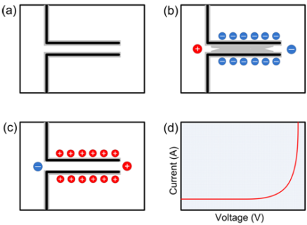
In this paper, we present a new self-switching diode (SSD) realized with a two-dimensional semiconductor hexagonal boron carbon-nitrogen (hBCN) monolayer. Channel length and width are 4.5 nm and 1.23 nm respectively. The device operation is simulated based on the Extended Huckel method and Nonequilibrium Green’s Function (NEGF) Formalism. The simulation results indicate non-linear I-V characteristics of the nano-diode and a current rectification ratio near 11250 that is higher than previous SSD structures reported before. Also, the effects of channel width on the electrical characteristics of SSDs are investigated. It can be found that the bandgap value of hBCN plays an important role in the modulation of current in the channel. Transmission pathways are provided under reverse and forward biases to show channel opening and pinch-off conditions. The results indicate that hBCN is a promising material for the realization of self-switching diodes (SSDs).
Graphical Abstract
Keywords
- NEGF
- Rectification Ratio
- Transmission Pathways.
- Extended Huckel Method
- Nanoscale Self Switching Diode
References
[1] Song A. M., Missous M., Omling P., (2003), Unidirectional electron flow in a nanometer-scale semiconductor channel: A self-switching device. Appl. Phys. Lett. 83: 1881-1883.
[2] Farhi G., Saracco E., Beerens J., (2007), Electrical characteristics and simulations of self-switching-diodes in SOI technology. Solid State Electron. 51: 1245-1249.
[3] Irshaid M. Y., Balocco C., Luo Y., (2011), Zinc-oxide-based planar nanodiodes operating at 50 MHz. Appl. Phys. Lett. 99: 092101-092103.
[4] Kettle J., Perks R. M., Holye R. T., (2009), Fabrication of highly transparent self switching diodes using single layer indium tin oxide. Electron Lett. 45: 79-81.
[5] Al-Dirini F., Hossain F. M., Nirmalathas A., (2014), Asymmetrically-gated graphene self-switching diodes as negative differential resistance devices. Nanoscale. 6: 7628-7634.
[6] Horri A., Faez R., (2019), Full-quantum simulation of graphene self-switching diodes. Chinese Phys. Lett. 36: 067202-067204.
[7] Al-Dirini F., Hossain F. M., Mohammed M. A., (2016), Monolayer MoS2 self switching diodes. J. Appl. Phys. 119: 044506-044510.
[8] Al-Dirini F., Hossain F. M., Mohammed M. A., (2015), Highly effective conductance modulation in planar silicene field effect devices due to buckling. Scientif. Rep. 5: 1-10.
[9] Cortes-Mestizo I. E., Briones E., Briones J., (2016), Study of InAlAs/InGaAs self-switching diodes for energy harvesting applications. Jpn. J. Appl. Phys. 55: 014304-014307.
[10] Ci L. J. , Jin C., Jariwala D., Wu D., Li Y., Srivastava A., Wang Z. F., Storr K., Balicas L., Liu F., Ajayan M. P., (2019), Atomic layers of hybridized boron nitride and graphene domains. Nature Mater. 9: 430-435.
[11] Zhu J., Bhandary S., Sanyal B., Ottosson H., (2011), Interpolation of atomically thin hexagonal boron nitride and graphene: Electronic structure and thermodynamic stability in terms of all-carbon conjugated paths and aromatic hexagons. J. Phys. Chem. C. 115: 10264-10271.
[12] Nehate S. D., Saikumar A. K., Prakash A., Sundaram K. B., (2020), A review of boron carbon nitride thin films and progress in nanomaterials. Mater. Today Adv. 8: 100106-100108.
[13] Ebrahimi M., Horri A., Sanaeepur M., Tavakoli M. B., (2020), Tight-binding description of graphene–BCN–graphene layered semiconductors. J. Comput. Electronics. 19: 62-69.
[14] Fiori G., Betti A., Bruzzone S., Iannaccone G., (2012), Lateral graphene–hBCN heterostructures as a platform for fully two-dimensional transistors. ACS Nano. 6: 2642–2648.
[15] Wolfsberg M., Helmholz L., (1952), The spectra and electronic structure of the tetrahedral ions MnO4−, CrO4−, and ClO4−. J. Chem. Phys. 20: 837-843.
[16] Al-Dirini F., Mohammed M. A., Hossain F. M., (2015), Tunable graphene nanopores for single biomolecule detection. Nanoscale. 8: 1-10.
[17] Guo J., Datta S., Lundstrom M., (2004), Toward multiscale modeling of carbon nanotube transistors. Int. J. Multiscale Comput. Eng. 2: 1-21.
[18] Naderi A., Abdi Tahne B., (2017), Band bending engineering in p-i-n all around carbon nanotube field effect transistor by multi-segment gate. Int. J. Nano Dimens. 8: 341-350.
[19] Dey D., De D., (2018), First principle study of structural and electronic transport properties for electrically doped zigzag single wall GaAs nanotubes. Int. J. Nano Dimens. 9: 134-144.
Additional Information
Volume 13 (2022)
Issue 4, November 2022
Page Numbers: 397-402

Article views: 6
Share: