Performance analysis of the novel Quad Gate Stacked nano-sheets FinFET device and its application in common source amplifier
Authors

Abstract
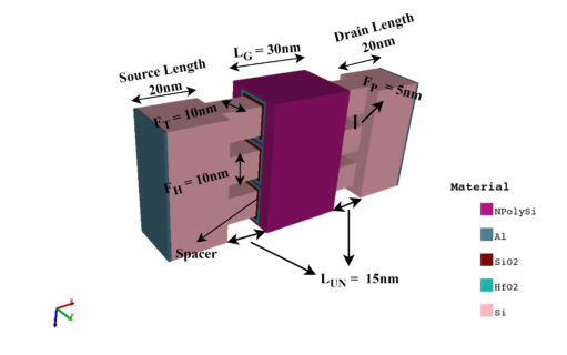
Stacked Nano-sheets FinFET device has evolved as a viable alternative to FinFET in designing low power circuits. The performance analysis of the novel Quad Gate Stacked Nano-sheets (QG-SNS) FinFET device and its comparison with FinFET and Stacked Nano-sheets devices have been carried out. QG-SNS FinFET device is designed on Cogenda TCAD tool at 30 nm technology node. Device simulation results indicate a steep sub-threshold slope of 26.7 mV/decade, ON current of is 1.0×10⁻⁵ A, and OFF current of is 9.85×10⁻¹⁴ A. The maximum cutoff frequency of 381 GHz is reported. The designed device shows higher early voltage and better device efficiency. Further, the performance-based comparative analysis of common source amplifier circuit designed with QG-SNS FinFET device is done with FinFET based amplifier. Circuit simulations have been performed utilizing the Look up table based Verilog-A model. Amplification of factor 1.93 has been achieved by QG-SNS FinFET based amplifier which is 60.8% better than that achieved by FinFET based amplifier, highlighting the capability of QG-SNS FinFET device for high frequency circuits having input signals of frequency 100 MHz. Average power dissipation and leakage power are reduced by 1.12 and 10-6 times respectively in QG-SNS FinFET based amplifier.
Graphical Abstract
Keywords
- Quad Gate FinFET
- OFF-Current
- Amplification
- Common Source Amplifier
- Leakage power
- Nano-sheet stacking
References
1. Auth, C., Allen, C., Blattner, A., Bergstrom, D., Brazier, M., Bost, M., Buehler, M., Chikarmane, V., Ghani, T., Glassman, T., Grover, B., Han, W., Hanken, D., Hattendorf, M., Hentges, P., Heussner, R., Hicks, J., Ingerly, D., Jain, P., Jaloviar, S., James, R., Jones, D., Jopling, J., Joshi, S., Kenyon, C., Liu, H., McFadden, R., McIntyre, B., Neirynck, J., Parker, C., Pipes, L., Post, I., Pradhan, S., Prince, M., Ramey, S., Reynolds, T., Roesler, J., Sandford, J., Seiple, J., Smith, P., Thomas, C., Towner, D., Troeger, T., Weber, C., Yashar, P., Zawadzki, K., Mistry, K. (2012). A 22nm high performance and low-power CMOS technology featuring fully-depleted tri-gate transistors, self-aligned contacts and high density MIM capacitors. Symposium on VLSI Technology (VLSIT). 131-132.https://doi.org/10.1109/VLSIT.2012.6242496
2. Ruhil Sh., Khanna V., Dutta U., Shukla N. K. (2021). A study of emerging semi-conductor devices for memory applications. Int. J. Nano Dimens. 12: 186-202.https://dx.doi.org/10.22034/ijnd.2021.680122
3. Al-Ameri, T., Georgiev, V. P., Adamu-Lema, F., Asenov, A. (2017). Simulation Study of Vertically Stacked Lateral Si Nanowires Transistors for 5-nm CMOS Applications. IEEE Journal of the Electron Devices Society. 5: 466-472. https://doi.org/10.1109/JEDS.2017.2752465
4. Badami, O., Caruso, E., Lizzit, D., Osgnach, P., Esseni, D., Palestri, P., Selmi, L. (2016). An Improved Surface Roughness Scattering Model for Bulk, Thin-Body, and Quantum-Well MOSFETs. IEEE Transactions on Electron Devices. 63: 2306-2312.https://doi.org/10.1109/TED.2016.2554613
5. Yeo, K. H., Suk, S.D., Li, M., Yeoh, Y., Cho, K.H., Yun, S., Lee, M.S., Cho, N., Lee, K., Hwang, D., Park, B., Kim, D.W., Park, D., Ryu, B. (2006). Gate-All-Around (GAA) Twin Silicon Nanowire MOSFET (TSNWFET) with 15 nm Length Gate and 4 nm Radius Nanowires. International Electron Devices Meeting, San Francisco. CA. pp. 1-4. https://doi.org/10.1109/IEDM.2006.346838
6. Ritzenthaler, R., Mertens, H., Pena, V., Santoro, G., Chasin, A., Kenis, K., Devriendt, K., Mannaert, G., Dekkers, H., Dangol, A., Lin, Y., Sun, S., Chen, Z., Kim, M., Machillot, J., Mitard, J., Yoshida, N., Kim, N., Mocuta, D., Horiguchi, N. (2018). Vertically Stacked Gate-All-Around Si Nanowire CMOS Transistors with Reduced Vertical Nanowires Separation, New Work Function Metal Gate Solutions, and DC/AC Performance Optimization. IEEE International Electron Devices Meeting (IEDM), San Francisco, CA, pp. 21.5.1-21.5.4.https://doi.org/10.1109/IEDM.2018.8614528.
7. Loubet, N., Hook1, T., Montanini, P., Yeung, C-W., Kanakasabapathy, S., Guillorn, M., Yamashita, T., Zhang, J., Miao, X., Wang, J., Young, A., Chao, R., Kang, M., Liu, Z., Fan, S., Hamieh, B., Sieg, S., Mignot, Y., Xu, W., Seo, S.-C., Yoo, J., Mochizuki, S., Sankarapandian, M., Kwon, O., Carr, A., Greene, A., Park2, Y., Frougier, J., Galatage, R., Bao1, R., Shearer, J., Conti, R., Song, H., Lee, D., Kong, D., Xu, Y., Arceo, A., Bi, Z., Xu, P., Muthinti, R., Li, J., Wong, R., Brown, D., Oldiges, P., Robison, R., Arnold, J., Felix, N., Skordas, S., Gaudiello, J., Standaert, T., Jagannathan, H., Corliss, D., Na, M.-H., Knorr, A., Wu, T., Gupta, D., Lian, S., Divakaruni, R., Gow, T., Labelle, C., Lee, S., Paruchuri, V., Bu, H., Khareet, M. (2017). Stacked nanosheet gate-all-around transistor to enable scaling beyond FinFET. Symposium on VLSI Technology, Kyot. pp. T230-T231.https://doi.org/10.23919/VLSIT.2017.7998183
8. Chu, C. L., Wu, K., Luo, G. L., Chen, B.Y., Chen, S. H., Wu, W. F., Yeh, W. K. (2018) Stacked Ge-Nanosheet GAAFETs fabricated by Ge/Si multilayer Epitaxy. IEEE Transactions on Electron Devices. 39: 1133–1136. https://doi.org/10.1109/LED.2018.2850366
9. Huang, Y. S., Lu, F. L., Tsou, Y. J., Ye, H. Y., Lin, S. Y., Huang, W. H., Liu, C. W. (2018). Vertically stacked strained 3-GeSn-Nanosheet pGAAFETs on Si using GeSn/Ge CVD epitaxial growth and the optimum Selective Channel release process. IEEE Transactions on Electron Devices. 39: 1274–1277.https://doi.org/10.1109/LED.2018. 2852775
10. Dasgupta, A., Parihar, SS., Kushwaha, P., Agarwal, H., Kao, M. Y., Salahuddin, S., Chauhan, Y. S., Hu, C. (2020). BSIM compact model of quantum confinement in advanced Nanosheet FETs. IEEE Transactions on Electron Devices. 67: 730–737.https://doi.org/10.1109/TED.2019. 2960269
11. Ajayan, J., Nirmal, D., Mathew, R., Kurian, D., Mohankumar, P., Arivazhagan, L., Ajitha, D. (2021). A critical review of design and fabrication challenges in InP HEMTs for future terahertz frequency applications. Materials Science in Semiconductor Processing. 128: 105753. https://doi.org/10.1016/j.mssp.2021.105753
12. Oliveira, A., Veloso, A., Claeys, C., Horiguchi, N., Simoen, E. (2020). Low-frequency noise assessment of vertically stacked Si n-channel Nanosheet FETs with different metal gates. IEEE Transactions on Electron Devices, 67: 4802–4807.https://doi.org/10.1109/TED.2020. 3024271
13. Yoon, J., Jeong, J., Lee, S., Baek, R. (2018). Systematic DC/AC performance benchmarking of Sub-7-nm node FinFETs and Nanosheet FETs. IEEE Journal of the Electron Devices Society. 6: 942–947.https://doi.org/10.1109/JEDS.2018.2866026
14. Nagy, D., Espiñeira, G., Indalecio, G., García-Loureiro, A.J., Kalna, K., Seoane, N. (2020). Benchmarking of FinFET, Nanosheet, and Nanowire FET Architectures for Future Technology Nodes. IEEE Access. 8: 53196-53202. https://doi.org/10.1109/ACCESS.2020.2980925
15. De Oliveira, A. V., Veloso, A., Claeys, C., Horiguchi, N., Simoen, E. (2020). Low–Frequency Noise in Vertically Stacked Si n–Channel Nanosheet FETs, IEEE Electron Device Letters. 41: 317-320.https://doi.org/10.1109/LED.2020.2968093
16. Ruhil, S., Dutta, U., Khanna, V. , Shukla, N.K. (2022). Design of a 30 Nm Novel 3-D Quad Gate Stacked Nano-Sheets FinFET, Silicon. 14: 11859–11868.https://doi.org/10.1007/s12633-022-01911-4
17. Ye, H.Y., Liu, C.W. (2020). On-current enhancement in TreeFET by combining vertically stacked Nanosheets and Interbridges. IEEE Electron Device Letters. 41: 1292–1295.https://doi.org/10.1109/LED.2020.3010240
18. Gaidhane, A. D., Pahwa, G., Dasgupta, A., Verma, A., Chauhan, Y. S. (2020). Compact Modeling of Surface Potential, Drain Current and Terminal Charges in Negative Capacitance Nanosheet FET including Quasi-Ballistic Transport. IEEE Journal of the Electron Devices Society. 8: 1168-1176.https://doi.org/10.1109/JEDS.2020.3019927
19. Sakib, F.I., Hasan, M.A., Hossain, M. (2020). Exploration of negative capacitance in gate-all-around Si Nanosheet transistors. IEEE Transactions on Electron Devices. 67: 5236–5242.https://doi.org/10.1109/TED. 2020.3025524
20. Veloso, A., Huynh-Bao, T., Matagne, P., Jang, D., Eneman, G., Horiguchi, N., Ryckaert, J. (2020). Nanowire & nanosheet FETs for ultra-scaled, high-density logic and memory applications. Solid State Electron. 168: 107736.https://doi.org/10.1016/j.sse.2019.107736
21. Biswas, K., Sarkar, A. & Sarkar, C.K. (2018). Fin shape influence on analog and RF performance of junction less accumulation-mode bulk FinFETs. Microsystem Technologies. 24: 2317–2324.https://doi.org/10.1007/s00542-018-3729-1
22. Kushwaha, P., Dasgupta, A., Kao, M-Y., Agarwal, H., Salahuddin, S., Hu, C. (2020). Design Optimization Techniques in Nanosheet Transistor for RF Applications. IEEE Transactions on Electron Devices,.67: 4515-4520.http://doi.org/10.1109/TED.2020.3019022
23. Vadthiya, N., Narware, P., Bheemudu, V., Bhukya, S. (2020). Investigation of Short Channel Effects (SCEs) and Analog/RF Figure of Merits (FOMs) of Dual-Material Bottom-Spacer Ground-Plane (DMBSGP) FinFET. Silicon. 12: 2283-2291. http://doi.org/10.1007/s12633-019-00322-2
24. Tayal, S., Ajayan, J., Joseph, L.M.I.L, Tarunkumar, J., Nirmal, D., Jena, B., Nandi, A. (2022). A Comprehensive Investigation of Vertically Stacked Silicon Nanosheet Field Effect Transistors: an Analog/RF Perspective. Silicon. 14: 3543–3550.https://doi.org/10.1007/s12633-021-01128-x
25. Mishra, A., Jha, K.K., Pattanaik, M. (2014). Parameter variation aware hybrid TFET-CMOS based power gating technique with a temperature variation tolerant sleep mode. Microelectron. J. 45: 1515-1521.https://doi.org/10.1016/j.mejo.2014.08.005
26. Kumar, A., Pattanaik, M., Srivastava, P., Jha, K.K. (2020). Reduction of Drain Induced Barrier Lowering in DM-HD-NA GAAFET for RF Applications. IET Circ Device Syst. 14: 270-275.https://doi.org/10.1049/iet-cds.2019.0306
27. Ruhil, S., Khanna, V., Dutta, U., Shukla, N.K. (2023). A 7T high stable and low power SRAM cell design using QG-SNS FinFET. AEU - International Journal of Electronics and Communications. 168: 154704.https://doi.org/10.1016/j.aeue.2023.154704
28. Zhang, Z., Jiang, X., Wang, R., Guo, S., Wang, Y., Huang, R. (2018). Extraction of Process Variation Parameters in FinFET Technology Based on Compact Modeling and Characterization. IEEE Trans. Electron Devices, 65: 847-854. https://doi.org/10.1109/TED.2018.2790083
29. Genius, 3-D Device Simulator, (2019), Version 1.9.3–18, Reference Manual, Cogenda Pvt. Ltd., Singapore.https://www.cogenda.com/ article/downloads
30. Palankovski, V., Kaiblinger-Grujin, G., Kosina, H., Selberherr, S. (1998). A Dopant-Dependent Band Gap Narrowing Model Application for Bipolar Device Simulation. In De Meyer, K., Biesemans, S. (Eds.), Simulation of Semiconductor Processes and Devices, Springer, Vienna.https://doi.org/10.1007/978-3-7091-6827-1_29
31. Vakkalakula, B. S., Vadthiya, N. (2021). Design and temperature assessment of junctionless nanosheet FET for nanoscale applications. Silicon. 14: 3823-3834.https://doi.org/10.1007/s12633-021-01145-w
32. Lin, H.C., Chou, T., Chung, C.C., Tsen, C.J., Huang, B.W., Liu, C.W. (2022). RF Performance of Stacked Si Nanosheet nFETs. IEEE Transactions on Electron Devices. 68: 5277-5283.https://doi.org/10.1109/TED.2021.3106287
33. Dutta U., Soni, M. K., Pattanaik, M. (2018). Simulation study of hetero dielectric tri material gate tunnel FET based common source amplifier circuit. International Journal of Electronics and Communications. 9: 2263–2270.https://doi.org/10.1016/j.aeue.2018.12.004
34. Prasad, M., Mahadevaswamy, U.B. (2021). Density gradient study on Junctionless stack Nano-sheet with stack gate oxide for low power application. IETE Journal of Research. 69: 1429-1436.https://doi.org/10.1080/03772063.2020.1869594
35. Jaiswal, S., Gupta, S. K. (2022). Digital Performance Analysis of Double Gate MOSFET by Incorporating Core Insulator Architecture. Silicon. 14: 10977-10987.https://doi.org/10.1007/s12633-022-01811-7
36. Sarkar, A., Kumar das, A., De, S., Sarkar, C.K. (2012). Effect of gate engineering in double-gate MOSFETs for analog/RF applications. Microelectronics Journal. 43: 873–882.https://doi.org/10.1016/j.mejo.2012.06.002
37. https://nanohub.org/resources/19195 Accessed 02/03/2022
38. http://bsim.berkeley.edu/models/bsimcmg/ Accessed 15/03/2022