Impact of nanometric buried Oxide layer on subthreshold swing and drain conductance of junctionless accumulation mode MOSFET for analog circuit applications
Authors

Abstract
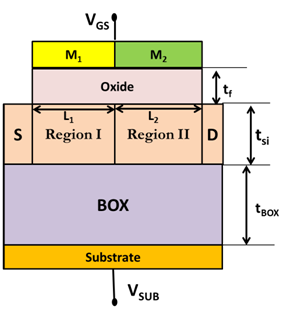
Drain conductance to drain current ratio is analytically investigated for junctionless accumulation mode MOSFET in presence of ultrathin buried oxide layer invoking the effect of conduction band tunnelling, within realistic range of dimensional configurations in nano regime. By taking into account the flatband voltage’s influence and the image charge effect at the oxide-semiconductor interface, subthreshold swing is evaluated over practical range of applied bias. Comparative study reveals that 42% and 36.5% improvements are found with published literature for the conductance to current ratio, whereas reduction of corresponding subthreshold swing is 51% and 34% respectively, considering all the data are computed w.r.t reported value of drain current; for identical structural and electrical configurations. Accuracy of the analytical findings is verified against that of the TCAD software’s numerical analysis. Result speaks in favour of the proposed candidate for amplifying low voltage signal in large scale along with suppression of leakage effect for analog amplifier applications.
Graphical Abstract
Keywords
- Subthreshold Swing
- Dielectric constant
- Nano-Dimension
- Buried Oxide layer
- Drain Conductance to Drain Current Ratio
- Doping Density
References
1. Iwai H., (2021), Past and Future of Micro-/Nano-electronics, IEEE 32nd Int. Conf. on Microelect. (MIEL), 12-14 September, Nis, Serbia. https://doi.org/ 10.1109/MIEL52794.2021.9569187
2. Sood H., Srivastava V. M., Singh G., (2018), Advanced MOSFET technologies for next generation communication systems - perspective and challenges: A review. J. Eng. Sci. Technol. Rev. 11: 180-195. https://doi.org/10.25103/jestr.113.25
3. Mishra B., Kushwah V. S., Sharma R., (2021), Power consumption analysis of MOSFET and Single electron transistor for inverter circuit. Materials Today: Proceed. 37: 6600-6604. https://doi.org/10.1016/j.matpr.2021.05.094
4. Maity N. P., Maity R., Baishya S., (2017), Voltage and oxide thickness dependent tunneling current density and tunnel resistivity model: Application to high-k material HfO2 based MOS devices. Superlatt. Microstruct. 111: 628-641. https://doi.org/10.1016/j.spmi.2017.07.022
5. Salehuddin F., Kaharudin K. E., Zain A. S. M., Yamin A. K. M., Ahmad I., (2014), Analysis of process parameter effect on DIBL in n-channel MOSFET device using L27 orthogonal array. AIP Conference Proceed. 1621: 322-328. https://doi.org/10.1063/1.4898486
6. Jaiswal, S., Gupta, S. K., (2023), Quantum mechanical study of double gate MOSFET with core insulator in channel for immune short channel effects. Silicon. 15: 3419-3430. https://doi.org/10.1007/s12633-022-02269-3
7. Rjoub A., Taradeh N. A., Mistarihi M. F. AI., (2014), Gate leakage current accurate models for nanoscale MOSFET transistors. IEEE 24th Int. Workshop on Power and Timing Modeling. Optimization and Simulation, Palma de Mallorca, Spain. https://doi.org/ 10.1109/PATMOS.2014.6951880
8. Baral K., Singh P. K., Kumar S., Singh A., Tripathy M., Chander S., Jit S., (2020), 2D analytical modelling of drain and gate-leakage currents of cylindrical gate asymmetric halo doped dual material-junctionless accumulation mode MOSFET. AEU – Int. J. Electron. Communic. 116: 153071. https://doi.org/10.1016/j.aeue.2020.153071
9. Cañada J., Yoshida Y., Miura H., Nakano N., (2020), An On-Chip scalable low power consumption high-voltage driver based on standard CMOS technology. IEEE Int. SoC Design Conf. Yeosu, South Korea. https://doi.org/10.1109/ISOCC50952.2020.9333001
10. Biswal S. M., Baral B., De D., Sarkar A., (2015), Analytical subthreshold modeling of dual material gate engineered nano-scale junctionless surrounding gate MOSFET considering ECPE. Superlatt. Microstruc. 82: 103-112. https://doi.org/10.1016/j.spmi.2015.02.018
11. Jiang C., Liang R., Wang J., Xu J., (2014), Analytical short-channel behaviour models of junctionless cylindrical surrounding-gate MOSFETs. Proc. Next-Generation Electronics (ISNE), Intl. Symp. https://doi.org/ 10.1109/ISNE.2014.6839323
12. Biswas K., Sarkar A., Sarkar C. K., (2016), Impact of fin width scaling on RF/Analog performance of junctionless accumulation-mode bulk FinFET. ACM J. Emerg. Technol. Comput. Sys. (JETC). 12: 1-12. https://doi.org/10.1145/2903143
13. Trivedi N., Kumar M., Haldar S., Deswal S. S., Gupta M., Gupta R. S., (2016), Analytical modeling simulation and characterization of short channel junctionless accumulation mode surrounding gate (JLAMSG) MOSFET for improved analog/RF performance. Superlatt. Microstruc. 100: 1263-1275. https://doi.org/10.1016/j.spmi.2016.11.009
14. Yadav S., Rewari S., Pandey R., (2022), Junctionless accumulation mode ferroelectric FET (JAM-FE-FET) for high frequency digital and analog applications. Silicon. 14: 7245-7255. https://doi.org/10.1007/s12633-021-01537-y
15. Vermeer M. L., Hueting R. J. E., Pirro L., Hoentschel J., Schmitz J., (2020), Interface states characterization of UTB SOI MOSFETs from the subthreshold current. IEEE Transact. Elect. Dev. https://doi.org/10.1109/TED.2020.3043223
16. Chander S., Sinha S. K., (2022), Effect of raised buried oxide on characteristics of tunnel field effect transistor. Silicon. 14: 8805-8813. https://doi.org/10.1007/s12633-022-01681-z
17. Jaafar H., Aouaj A., Bouziane A., Iñiguez B., (2020), A compact model of transconductance and drain conductance for DMG-GC-DOT cylindrical gate MOSFET. Int. J. Reconfig. Embed. Sys. 9: 34-41. http://doi.org/10.11591/ijres.v9.i1.pp34-41
18. Batwani H., Gaur M., Kumar M. J., (2009), Analytical drain current model for nanoscale strained-Si/SiGe MOSFETs. Int. J. Comput. Mathemat. Electric. Electron. Eng. 28: 353-371. https://doi.org/10.1108/03321640910929263
19. Wagaj S., Chavan Y., Patil S., (2016), A two-dimensional analytical model and simulation for dual material gate junctionless transistor, advances in intelligent systems research, proceedings of the International Conference on Communication and Signal Processing 2016 (ICCASP 2016). https://doi.org/10.2991/iccasp-16.2017.56
20. Sadjadi M. A., Sadeghi B., Zare K., (2007), Natural bond orbital (NBO) population analysis of cyclic thionylphosphazenes, [NSOX (NPCl2)2]; X = F (1), X = Cl (2). J. Mol. Str.:THEOCHEM. 817: 27-33. https://doi.org/10.1016/j.theochem.2007.04.015
21. Karimi Pashaki Y., Sedigh Ziabari S. A., Eskandarian A., Rahnamaei A., (2023), Numerical optimization of threshold voltage and off-current of a nano-scale symmetric double gate MOSFET based on the genetic algorithm: Various strategies compatible with device applications. Int. J. Nano Dimens. 14: 91-102. https://doi.org/10.22034/ijnd.2022.1963798.2166
22. Priya A., Srivastava N. A., Mishra R. A., (2018), Perspective of buried oxide thickness variation on triple metal-gate (TMG) recessed-S/D FD-SOI MOSFET. Adv. Elect. Electron. Eng. 16: 380-387. https://doi.org/10.15598/aeee.v16i3.2797
Additional Information
Volume 15 (2024)
Issue 2, March 2024
Page Numbers: 152412 (1-9)

Article views: 62
Share: