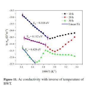
Tungsten doped Barium Titanate (BT) with composition BaW0.05Ti0.95O3 (BWT) were prepared by using ball milling technique for different hours (10h, 20h and 30h). In the present paper, the microstructural, dielectric and impedance studies are discussed. The microstructural studies using XRD data reveals the formation of single phased tetragonal structure and perovskite structure. The dielectric properties […]
AbstractMesoporous silicon (mesoPSi) layers fabricated by the photoelectrochemical etching (PECE) method in hydrofluoric acid (HF) are active as carbon monoxide gas sensors. The modified porous silicon (PSi) can be used with noble metals to manufacture an effective gas sensor. Embedded gold, platinum, and palladium nanoparticles Au, Pt, and Pd-NPs could modify the surface morphology of […]
AbstractIn this experimental study, a 1.5-kJ plasma focus device of Mather type was employed to grow titanium aluminum nitride (TiAlN) coatings at room temperature on 316 stainless steel sub-layer. The anode of the device was made of Titanium and Aluminium. A mixture of N2 and Ar gases was used as the work gas for TiAlN […]
AbstractThree steps anodization process is used to synthesize highly ordered and uniform multilayered titanium oxide (TiO2) nanotubes and effect of different anodization voltages are studied on their physical properties such as structural, morphological and optical. The crystalized structure of the synthesized tubes is investigated by X-ray diffractometer analysis. To study the morphology of the tubes, […]
AbstractCadmium telluride (CdTe) is a p-type II-VI compound semiconductor, which is an active component for producing photovoltaic solar cells in the form of thin films, due to its desirable physical properties. In this study, CdTe film was deposited using the radio frequency (RF) magnetron sputtering system onto a glass substrate. To improve the properties of […]
AbstractAl-doped ZnO (Al/ZnO) thin film is a promising alternative to an ITO electrode in solar cell applications due to its low price, non-toxicity and other promising properties. In this paper, Al/ZnO thin films at different substrate temperatures were deposited on glass substrates as transparent conducting (TCO) films by DC magnetron sputtering. The effect of substrate […]
AbstractZnO nanoparticles were synthesized from chitosan and zinc chloride by a precipitation method. The synthesized ZnO nanoparticles were characterized by Fourier transform infrared spectroscopy, X-ray diffraction peak profile analysis, Scanning electron microscopy, Transmission electron microscopy and Photoluminescence. The X-ray diffraction results revealed that the sample was crystalline with a hexagonal wurtzite phase. We have investigated […]
AbstractEuropium-doped gallium oxide (Ga2O3:Eu) thin films have successfully been grown using direct current magnetron sputtering by means of Eu concentration variation. Energy-dispersive X-ray spectroscopy spectra indicate gallium, oxygen, and europium elements as the growing films’ chemical compositions. Based on scanning electron microscopy images, the morphology of Ga2O3:Eu thin film is seemingly like a granulated nano-size […]
AbstractA 2.2-kJ Mather type plasma focus device charged at 18 kV was used to deposit titanium nitride on 304 type stainless steel substrates. The plasma focus device is fitted with solid titanium anode and operated with nitrogen as the filling gas. The process of deposition was done at room temperature, and samples were deposited at […]
