The next generation of photonics and nano-optical devices may be based on two-dimensional(2D) transition metal dichalcogenides (TMDs). In this research, molybdenum diselenide (MoSe2) nanosheets, as one important member of TMDs, have been synthesized by the solvothermal method and characterized through XRD patterns, SEM, and TEM images. Nanosheets were found to have a hexagonal phase based […]
This paper addresses the annealing temperature effect on nanostructure and phase transition of copper oxide thin films, deposited by PVD method on glass substrate (at 110 nm thickness) and post annealed at different temperatures (200-400°C) with a flow of 1 cm3s-1 Oxygen. The X-ray diffraction (XRD) was employed for crystallographic and phase analyses, while atomic […]
This paper reports the correlation between film thickness, nanostructure and DC electrical properties of copper thin films deposited by PVD method on glass substrate. X-ray diffraction (XRD) and atomic force microscopy (AFM) were used for crystallography and morphology investigation, respectively. Resistivity was measured by four point probe instrument, while a Hall effects measurement system was […]
In this study, TiO2 and ZnO nanofilms were prepared by sol-gel spin-coating method. Nanofilms were characterized by X-ray Diffraction (XRD), Energy Dispersive Analysis of X-ray (EDX), Scanning Electron Microscopy (SEM) and Field Emission Scanning Electron Microscopy (FE-ESM). Structural and morphological properties of nanofilms were investigated. The average crystalline size of TiO2 and ZnO nanoparticles which […]
ZnO thin film of 80 nm thickness was deposited by the sol-gel spin coating method on SiO2/Si substrate and subsequently post-annealed at 500°C with a flow of oxygen for 60 min. Crystallographic structure of the sample was characterized by X-ray diffraction (XRD) method while a field emission scanning electron microscope (FESEM) was used to investigate […]
In this study, different samples of Niobium and Vanadium co-doped titania thin films (5-10-15 mol% Nb and 5-10-15 mol% V) were prepared via sol−gel dip coating method, using niobium chloride as niobium precursor, ammonium metavanadate as vanadium precursor, and titanium (IV) butoxide (TBT) as titanium precursor. The effects of doping amount on the structural, optical, […]
With attention to the thin film structure of colloidal quantum dot solar cells, in this paper in order to improvement of active layer absorption of them, we have proposed the use of nanostructure pattern for enhancement of their performance. For this purpose we have presented suitable nano hemisphare patterns in colloidal quantum dot solar cells […]
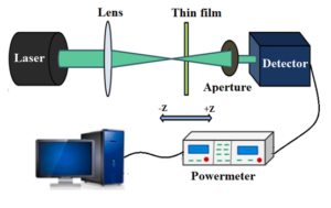
In this article, the growth kinetic and optical property of amorphous carbon (a-C) nanolayers deposited by ion beam sputtering deposition technique on glass substrates are investigated. The atomic force microscopy is used to measure the variation of surface roughness versus deposition time. According to the calculations, the roughness of thin films increases during the growth […]