Department of Computer Science and Engineering, Maharishi University of Information Technology, Lucknow, Uttar Pradesh, 226013, IN
Department of Electronics and Communication Engineering, Bharat Institute of Engineering and Technology, Hyderabad, 501510, IN
Department of Electronics and Telecommunication, Veer Surendra Sai University of Technology, Burla, 768018, IN
Abstract
Quantum technology has an attractive application nowadays for its minimizing the energy dissipation, which is a prominent part of any system-level design. In this article, the significant module of a multiplexer, an extended to
n
:1 is framed with prominent application in the control unit of the processor. The proposed multiplexer modules are framed by the algorithm, which is extended perspective based. Further, quantum cost and gate count are less to ensure the efficient quantum computing framed. In addition, the QCA computing framework is an attempt to synthesize the optimal primitives in conservative reversible multiplexer in nano-electronic confine application. The developed lemmas is framed to prove the optimal parameters in the reversible circuit. Compared with existing state-of-art-works, the proposed modular multiplexer, the gate count, quantum cost and unit delay are optimal.
Introduction
The complementary metal-oxide semiconductor (CMOS) circuit design in the nanometer scale range has primary limitations such as MOS transistor width (
W
), length (
L
) and short channel effect that cause degradation of the device performance [
1
]. To overcome the problems the research moved towards nanotechnology [
2
]. Recently quantum-dot cellular automata (QCA) general theorems promise the principle of low power, high device density, high switching speed and high operating frequency (THz) [
3
]. On the other hand, reversible logic has a popular field in the area of digital logic that can perform computing with almost zero power consumption [
4
]. Energy dissipation is a significant factor in digital logic circuits. According to Landauer, the single bit of data lost generates
KT
ln2 = 0.017 eV of heat energy, where
K
is Boltzmann’s constant and
T
= 300 K is the absolute temperature [
5
]. Bennett proved that a zero power dissipation in a digital circuit is likely only if the circuit is designed for reversible logic gates [
6
]. In low power area, the reversible logic technique has an emerging area in Nano-electronics and quantum computing. In specific quantum, circuits are nanometric scale and high computation speed. Since they involve tiny size particle (known as qubits) and exist in the atomic scale level [
7
]. The advantage of reversible logic is that quantum computing is made of this method. Moreover, reversible logic is top-level emerging technologies, which process high-speed computing, low power, and nanometric scale [
8
]. Initially, the conservative based circuits are designed that emphasis on controlling the fault, which in turn increase the reliability of the circuits [
9
]. The second most important factor is a cost, which basic part of the quantum cost. If we focus on these two points, then the efficiency of the circuit will be enhanced. The novelty of this work is to design the circuits by combining all the above two factors.
Among all digital integrated circuits, multiplexer circuits are the fundamental part, which is embedded in the module part of the control unit of the processor. More appropriately, the control unit of the processor consists of the multiplexer [
9
]. After reviewing the state-of-the-art work in this area, it can be conceived that a significant amount of research has been done in this domain besides few works targets the conservative approach, combined quantum logic circuit, and QCA framework [
4
,
7
,
10
,
11
,
12
,
13
–
14
]. The circuit by the authors in [
7
] such as 2:1 multiplexer was presented by MX-cqca gate using the conservative, but it is non-reversible. This multiplexer circuit has some constraints such as the modular approach cannot be developed for higher-order multiplexer, quantum circuit not realized because it is non-reversible. The main drawback of existing multiplexer in literature is it’s not conservative reversible logic based, many researchers synthesize effort for optimizing the QCA parameters such as cell count, area and latency as [jcel1, jcel2]. The tendency to use such non-conservative QCA multiplexer is not fault tolerance and its high error rate too [
15
,
16
]. After reviewing all the state-of-art-work, it can be analyzed that our proposed circuits have some speciality such as low-cost metric parameters (gate count, garbage outputs, and quantum cost) and conservative reversible logic based. In the more specific multiplexer, design approach extended for n-bit input using the developed algorithm. Further QCA layout implementation of proposed multiplexer has been constructed which appropriate to current Nano-electronics confine application.
Most of the above literature paper circuits discussed above not optimize, there is utilizing more quantum cost, not conservative approach and no quantum equivalent circuit of design. This means these designs are not cost-effective in terms of quantum cost and it is not conservative. However, the introduced design of multiplexer achieve optimal value of parameters and the performance is also studied by expanding the quantum equivalent circuit for the proposed design.
This work proposes low quantum cost-based conservative reversible multiplexer. The outlines of the workaround proposed circuits can be pointed out as follow.
We design a conservative, reversible
m
:1 type multiplexer using existing R-CQCA gate. The presented quantum circuit shows the circuit is more cost-effective regarding quantum cost as compared to existing ones.
We present the smaller QCA robust structure of multiplexer, and the simulation outcomes specify the correct functionality for the minimum clock cycle delay.
We design a cost-effective, conservative reversible multiplexer based on proposed algorithm.
We design a 2:1 multiplexer layout through QCADesigner tool, which provide the 0.25 s latency and 0.24 µm
2
area.
We synthesize the multiplexer based on algorithm it expand to
n
:1 multiplexer also and it helpful for ALU, and control unit of processor design.
This section, we have presented the basic terminology such as reversible logic, conservative, reversible logic and QCA that are related to this work. Basic terminologies have been reviewed in state-of-the-art work as per [
17
,
18
,
19
–
20
].
Definition 2.1
The reversible gate should have the equal number of inputs
Iv
(
A0
,
A1
,…
An
) and outputs
Ov
(
B0
,
B1
,…
Bn
) and the bijective mapping at the same time. Figure
1
a drawn the reversible gate.
Fig. 1
An
n
×
n
architecture of reversible gate
Definition 2.2
A conservative, reversible gate is a hamming weight of inputs and outputs is equal [
8
], which is shown in Fig.
1
b. More appropriately, it can be drawn in Eq. (
1
).
A1⊕A2⊕…An⟷bijectiveB1⊕B2⊕…Bn
Definition 2.3
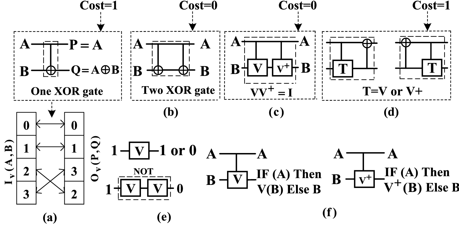
The significant cost-metric parameter for reversible logic is quantum cost. Any reversible gate can be decomposed into 1 × 1 and 2 × 2 gates such as CNOT,
V
and
V+
gates (called quantum primitive gates). The CNOT gate is depicted in Fig.
2
a and the quantum cost calculation for some basic structures are depicted in Fig.
2
b–e. The cost is calculated by counting the total primitives gates [
7
]. The controlled
V
and
V+
gate are depicted in Fig.
2
f. In the controlled
V
gate when the control input
A
= 1, implies
Q
=
V
(
B
), that
V
is synthesized by Eq. (
2
). When
A
= 0, implies
Q
= B, where
A
and
B
are inputs and
Q
is the output. The
V
and
V+
gates have some basic properties that drawn in Eqs. (
3
) and (
4
).
V=i+121-i-i-1V×V=V+×V+=NOTV+×V=V×V+=I
Fig. 2
Basic of quantum cost
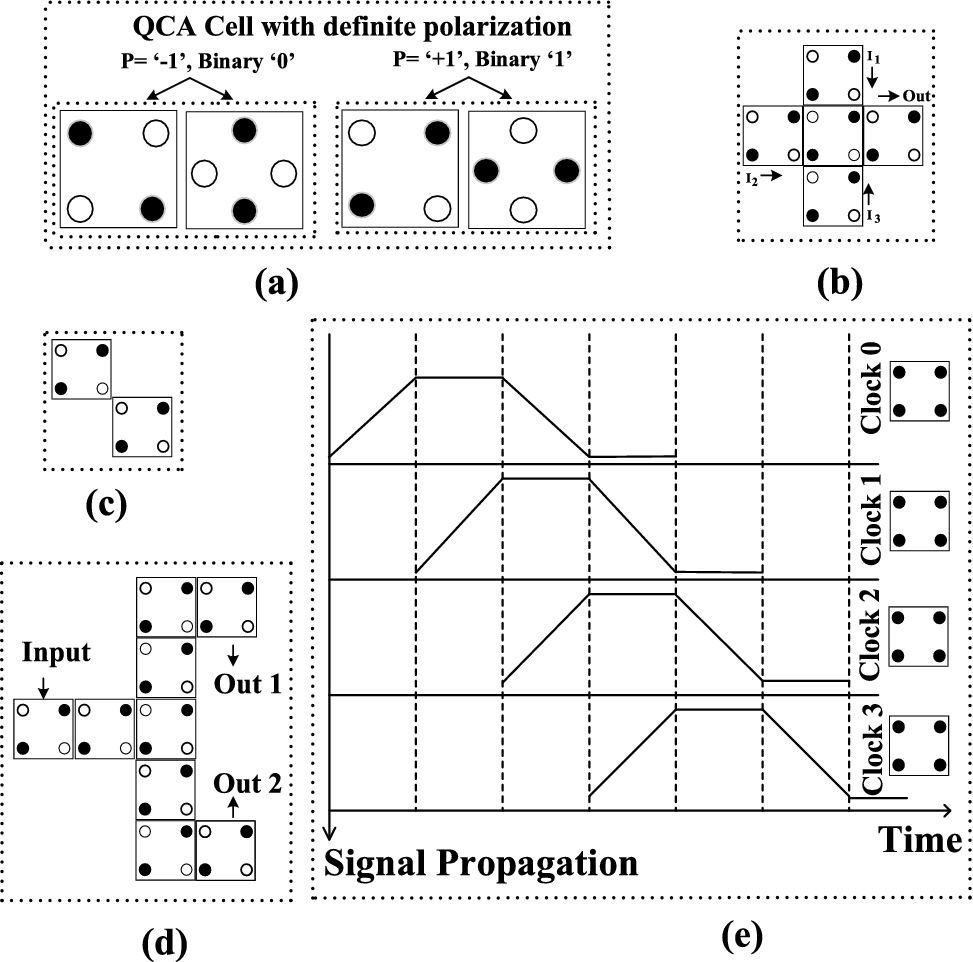
Definition 2.4
In QCA cell has a quantum dot, with a four number. The shape of quantum-dot is circular with a specified diameter of 10 nm, and each dot is situated within a neighbor radius of 20 nm. Whether two extra electrons are situated in existing two quantum dots, and the arrangement is always in a diagonal way. The formed QCA cell can be a definite polarization (Fig.
3
a). The majority gate, inverter, fan-out concept, and clock are depicted in Fig.
3
b–d, respectively. The binary value stored in the QCA cell can be defined by polarization. The polarization expression is drawn by Eq. (
5
).
P=(σ1+σ3)-(σ2+σ4)σ1+σ2+σ3+σ4
Fig. 3
QCA fundamentals
a
QCA cell,
b
majority gate,
c
smaller robust inverter,
d
fan out and
e
clocking
Definition 2.5
QCA has four clock zones; the utility is to control the information flow. Four clock zones are categories by four phase (Switch, Hold, release and relax). Clock zone is shown in Fig.
3
e.
Definition 2.6
The kink energy is the difference between the maximum and minimum energy. Whereas maximum energy exist when the two cells have opposite polarization and have the minimum energy when they have the same polarization. The kink energy is drawn by Eq. (
6
). Whereas the electrostatic energy of a circuit is formed by considering two cells (named cell a and cell b) with polarization (called
Pa
and
Pb
) side by side, is drawn by Eq. (
7
).
Ekink=EPm≠Pnm,n-EPm=Pnm,nEm,n=14πε0Σk=14Σl=14qkmqln|rkm-rln|
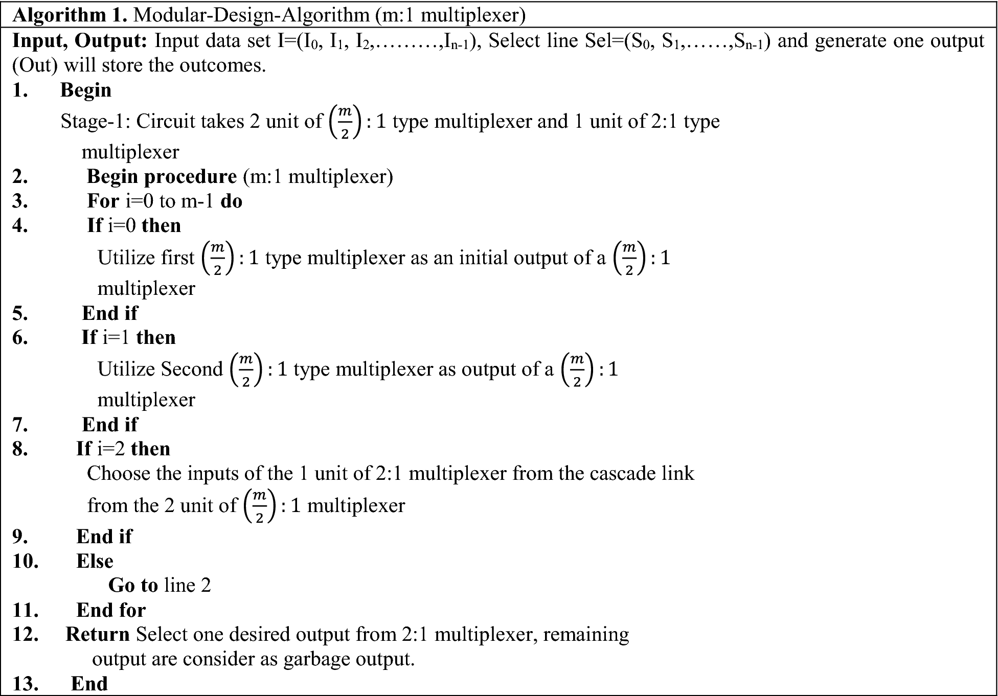
Proposed multiplexer based on R-CQCA gate
To test the circuit, the conservative logic claims to have cost-efficient application in reversible logic circuits. In fact, the conservative feature is the prominent part of testing reversible gates [
21
]. Hence, to achieve a low error rate and testing feature, the conservative, reversible technique would truly be remarked as the useful feature for construction digital logic integrated circuits. The conservative, reversible logic useful in QCA technique since it addresses the cost-efficient concern, such as: reducing cell complexity, reducing delay, layout area, and power [
14
].
In this paper, a novel multiplexer, circuit have been constructed by existing reversible gate [
21
]. The R-CQCA gate is utilized for the multiplexer circuit. In “
Modular approaches to design a multiplexer
” section, multiplexer circuits are presented.
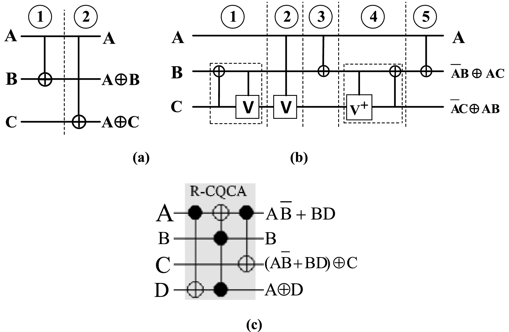
Existing conservative, reversible gates
The two popular existing conservative, reversible gate is F2G, FRG and R-CQCA. In F2G input vector is
Iv
the output vector
Ov
and they are set by
Iv(A,B,C)
and
Ov=(A,A⊕B,A⊕C)
. In FRG input and output vector are set as
Iv(A,B,C)
and
Ov=(A,A¯B+AC,A¯C+AB)
. The other conservative, reversible gate is R-CQCA; it is popular due to its low value of quantum cost [
21
]. The quantum cost of F2G, FRG, and R-CQCA are 2, 5 and 6, respectively. Conservative, reversible R-CQCA gate is used for synthesized the multiplexer in this work. The quantum equivalent circuit of F2G, FRG, and R-CQCA is depicted in Fig.
4
a–c respectively.
Fig. 4
Existing conservative, reversible gate quantum circuit
a
F2G,
b
FRG and
c
R-CQCA
Modular approaches to design a multiplexer
In the computational field, the multiplexer is used to select the particular data [
9
]. The 2:1 Mux design is constructed using 1 × R-CQCA, and its unit delay is 1. The schematic and quantum circuit is well furnished by the 2:1 mux as depicted in Fig.
5
a. In the 2:1 mux consist of one select line (Sel), two input information (
I0
,
I1
) and one required output (Out). The output is synthesized by
Out=Sel¯(I0)+Sel(I1)
. When Sel = 0 then output data line connect to
I0
and for Sel = 1 output connect to
I1
.
Fig. 5
Reversible multiplexer
In a modular approach, the generic unit of 2:1 mux can be employed for 4:1 Mux, a simplified three unit of 2:1 mux version is employed for the design of 4:1 mux. The corresponding schematic and quantum presentation of 4:1 mux are shown in Fig.
5
b. However, based on the circuit configuration used for binary data, select inputs by select line inputs is drawn in Table
1
.
Table 1
4:1 Multiplexer data output
Select line inputs
Intermediate outputs
Data output
Sel1
Sel2
X
Y
Out
0
0
I0
I2
I2
0
1
I0
I2
I0
1
0
I1
I3
I3
1
1
I1
I3
I1
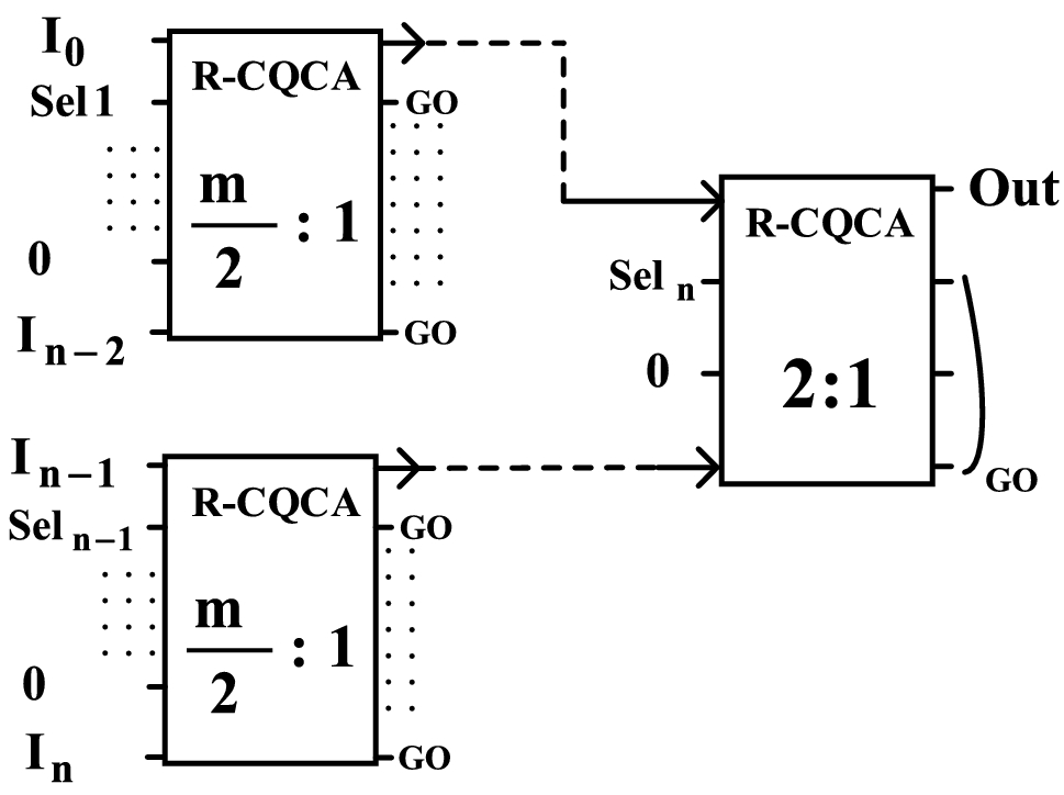
Using the two units of 4:1 Mux and one unit of 2:1 mux we can accomplish the 8:1 mux, whose construction is shown in Fig.
5
c. A straightforward approach for multiplexer design is adopted in
m
:1 mux design. Thus, the design of
m
:1 mux has at least two unit of
m2:1
mux in addition one unit of 2:1 mux. A complete construction for the execution of
m
:1 multiplexer is depicted in Fig.
6
. Thus, according to the modular approach of multiplexer, lower bound reversible parametric analysis of the number of date inputs m is given by Lemma
1
. A construction algorithm of
m
:1 multiplexer is drawn in Algorithm 1. According to 8:1 multiplexer circuit, their computation process of data inputs is drawn in Table
2
.
Fig. 6
Modular design of
m
:1 multiplexer
Table 2
8:1 Multiplexer data output
Select line inputs
Intermediate outputs
Data output
Sel1
Sel2
Sel3
X
Y
Z
W
P
Q
Out
0
0
0
I0
I2
Y
I4
I6
P
I2
0
0
1
I0
I2
Y
I4
I6
P
I6
0
1
0
I0
I2
X
I4
I6
W
I0
0
1
1
I0
I2
X
I4
I6
W
I4
1
0
0
I1
I3
Y
I5
I7
P
I3
1
0
1
I1
I3
Y
I5
I7
P
I7
1
1
0
I1
I3
X
I5
I7
W
I1
1
1
1
I1
I3
X
I5
I7
W
I5
Lemma 1
An m:1 multiplexer cascading link by the R-CQCA can be synthesized by (m − 1) be the minimum gate count (GC) and constant input (CI), 2(m − 1) + log2mbe the garbage output (GO) and 4(m − 1) quantum cost (QC)
Proof
The construction of
m
:1 multiplexer consists of
m2:1
multiplexer and single 2:1 multiplexer. Hence the minimum GC and CI for 2:1, 4:1, 8:1 and
m
:1 type of multiplexer is
GC2:1mux=CI2:1mux=1=2-1
Hence above equation hold for
m
= 2.
GC4:1mux=CI2:1mux=3=4-1GC8:1mux=CI2:1mux=7=8-1
Assume that the Eq. (
8
), (
9
) and (
10
) supports for
m
=
n
. Therefore, an
m
:1 multiplexer can be synthesized by (
m
− 1) gate count.
The GO rise by a 2:1, 4:1, 8:1 and
m
:1 type of multiplexer as drawn by Eqs. (
11
), (
12
) and (
13
)
GO2:1mux=3=22-1+log22
Hence above equation hold for
m
= 2.
GO4:1mux=8=24-1+log24GO8:1mux=17=28-1+log28
As a mathematical induction, the least 2(
m
− 1) +
log2m
garbage output for
m
:1 type of multiplexer.
A 2:1, 4:1, 8:1 type of multiplexer requires 4, 12 and 28 quantum cost. The quantum cost of
m
:1 multiplexer synthesize by induction as below Eqs. (
14
), (
15
) and (
16
)
QC2:1mux=4=2-1×4
Hence above equation hold for
m
= 2.
QC4:1mux=12=4-1×4QC8:1mux=28=8-1×4
Therefor a
m
:1 multiplexer hold the 4(
m
− 1) relationship for QC.
Design of conservative reversible multiplexer gate in QCA
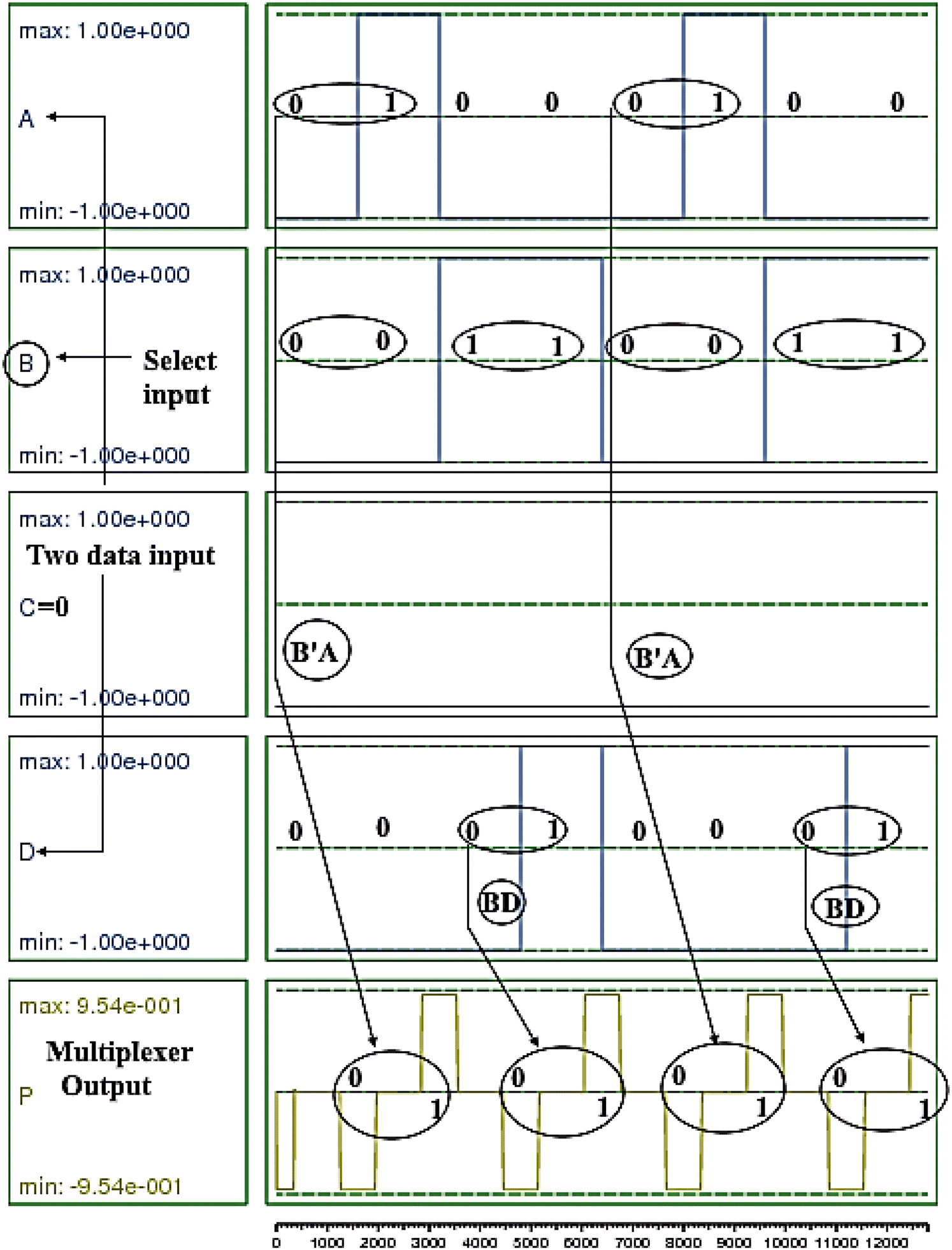
To judge the efficiency of the proposed R-CQCA, the cell layout in QCA Designer is considered. The cell layout of R-CQCA is depicted in Fig.
7
. The Bistable-approximation engine is used for outcomes verification. In Fig.
8
, it visualizes the results. It depicts that the results are strong polarization value of different input combinations. The beginning output
P
is acquired after 0.25 clock cycle delay. The third (
R
) and fourth (
S
) outputs are acquired after 1 clock cycle delay. Using cell layout and simulation, outcomes 3 important features (complexity, speed, and area) are extracted from this proposed layout, which is shown in Lemma
2
.
Fig. 7
Cell layout of R-CQCA
Fig. 8
Simulation result of 2:1 multiplexer using R-CQCA
Lemma 2
The maximum latency required to synthesize a 2:1 multiplexer using simulation outcomes is 0.5.
Proof
In the 2:1 multiplexer, cell layout is depicted in Fig.
7
. The outcomes are verified under the bistable approximation model with default parameters in QCA Designer. The simulation outcomes elucidate that when select input
B
= (0, 0) the outcomes
P
= (0, 1), appear after 0.5 latency i.e. input
A
= (0,1) is selected and sent to output node
P
. When to take the inputs
B
= (1, 1) the outcomes as
P
= (0, 1) i.e. input
D
= (0,1) is routed to output node
P
. Therefore, it is observe that ancilla inputs play an important role to get the output of multiplexer. Maximum latency of 2:1 multiplexer is 0.5, as depicted in simulation result in Fig.
8
. Hence, maximum 0.5 latency is utilized for projects in 2:1 multiplexer.
Table 4 presents the comparative analysis of multiplexer
Table
3
shows the proposed reversible primitives of multiplexer circuits. Table
4
presents a comprehensive comparison between the existing and proposed multiplexer circuit regarding reversible metrics such as gate count, garbage outputs, quantum cost and conservative feature. Recent existing work in [
4
,
7
,
12
,
13
] have some reversible metrics, the proposed modular approach based multiplexer has the capability of optimizing all reversible metrics. The comparative analysis table depicted in Table
5
.
Table 3
Performance metrics analysis of proposed multiplexer
Multiplexer
Metrics
2:1
1 QC (R-CQCA) = 6
1 GO (R-CQCA) = 4
1 CI (R-CQCA) = 1
1 UD (R-CQCA) = 1
4:1
3 QC (R-CQCA) = 3 × 6 = 18
3 GO (R-CQCA) = 2 + 3 + 3 = 8
3 CI (R-CQCA) = 1 + 1 + 1 = 3
3 UD (R-CQCA) = 3
8:1
2 QC (4:1 mux) + 1 QC (R-CQCA) = 2 × 18 + 6 = 42
2 GO (4:1 mux) + 1 GO (R-CQCA) = (6 + 8) + 3 = 17
2 CI (4:1 mux) + 1 CI (R-CQCA) = 2 × 3 + 1 = 7
2 UD (R-CQCA) = 2 × 3 + 1 = 7
Table 4
Comparative analysis results of multiplexer design in QCA
Design
Reversible
Cell count
Majority gate
Inverter
Latency
Area (µm2)
Existing [3]
No
246
11
4
1.25
0.25
Existing [10]
No
124
9
9
2
0.25
Existing [11]
No
154
3
4
1
0.15
Existing [14]
No
23
3
1
1
0.02
New
Yes
177
9
1
0.25
0.24
Table 5
Comparison between the proposed and existing multiplexer
Type
[4]
[7]
[12]
[13]
Proposed
2:1
GC
1
1
1
1
1
GO
2
2
1
2
3
QC
4
5
4
4
6
Conservative
No
Yes
No
No
Yes
Equivalent quantum circuit
No
No
No
No
Yes
4:1
GC
3
3
3
6
3
GO
5
5
5
10
8
QC
12
15
12
28
12
Conservative
No
Yes
No
No
Yes
Equivalent quantum circuit
No
No
No
No
Yes
m:1
GC
(m − 1)
3n
–
–
(m − 1)
GO
(m − 1) + log2m
4m + 1
–
–
2(m − 1) + log2m
QC
4(m − 1)
15m
–
–
4(m − 1)
Conservative
No
Yes
–
–
Yes
Conclusion
This work targets the basic factor such as cost-efficient solutions for nano-electronics based confine application, which has been successfully presented in this article. The cost-efficient conservative reversible multiplexer has been discussed and introduced successfully. The synthesizer circuits discussed in this paper is new and has achieved the target results. In fact, we have explored our proposed reversible gate R-CQCA in the dissimilar type of circuits such as multiplexer. First, the modular approach for multiplexer circuits, it presents better parameters as compared to existing ones. We have proven the reliability of multiplexer by lemmas. The inevitable optimal parameters
m
:1 mux is
2m-1+log2m
garbage outputs and 4(
m
− 1) quantum cost. The entire circuits work around R-CQCA and its aim is to optimize the quantum cost. The R-CQCA has only 6 quantum cost. Proposed multiplexer is analyzed on QCADesigner simulator. In further analysis has been included to determine the impact of R-CQCA in QCA technology. It is found that 0.25 latency, 0.24 µm
2
area, 177 cell complexity. The proposed dissimilar type of circuit will facilitate the coverage of low reversible parameters, QCA logic computing, and classification of QCA parameters such as complexity (cell count), speed (latency) and area usages.
Publisher's Note
Springer Nature remains neutral with regard to jurisdictional claims in published maps and institutional affiliations.
References
Singh et al. (2018) Implementation of Non-restoring Reversible Divider Using a Quantum-Dot Cellular Automata (pp. 459-469) Springer Singapore
Sridharan and Pudi (2015) Springer
Chabi et al. (2012) New modules for quantum-dot cellular automata AND & OR gates Can 3(5) (pp. 200-208)
Sen et al. (2014) Modular design of testable reversible ALU by QCA multiplexer with increase in programmability 45(11) (pp. 1522-1532) 10.1016/j.mejo.2014.08.012
Landauer (1961) Irreversible and heat generation in the computing process (pp. 183-191) 10.1147/rd.53.0183
Bennett (1973) Logical reversibility of computation (pp. 525-532) 10.1147/rd.176.0525
Thapliyal and Ranganathan (2010) Design of reversible sequential circuits optimizing quantum cost, delay, and garbage outputs 6(4)
Angizi et al. (2015) Designing quantum-dot cellular automata counters with energy consumption analysis 39(7) (pp. 512-520) 10.1016/j.micpro.2015.07.011
Jamal et al. (2013) An efficient approach to design a reversible control unit of a processor 3(4) (pp. 286-294)
Unknown ()
Unknown ()
Malhotra et al. (2014) Efficient design of reversible multiplexers with low quantum cost 4(7) (pp. 20-23)
Syamala and Tilak (2010) Synthesis of multiplexer and demultiplexer circuits using reversible logic 4(3) (pp. 34-38)
Sen et al. (2015) Towards modular design of reliable quantum-dot cellular automata logic circuit using multiplexers (pp. 42-54) 10.1016/j.compeleceng.2015.05.001
Rashidi et al. (2016) High-performance multiplexer architecture for quantum-dot cellular automata 15(3) (pp. 968-981) 10.1007/s10825-016-0832-3
Sabbaghi-Nadooshan and Kianpour (2014) A novel QCA implementation of MUX-based universal shift register 13(1) (pp. 198-210) 10.1007/s10825-013-0500-9
Lent and Tougaw (1997) A device architecture for computing with quantum dots 85(4) (pp. 541-557) 10.1109/5.573740
Pal et al. (2018) Realization of Basic Gates Using Universal Gates Using Quantum-Dot Cellular Automata (pp. 541-549) Springer Singapore 10.1007/978-981-10-6890-4_53
Sasamal et al. (2018) Efficient design of reversible logic ALU using coplanar quantum-dot cellular automata 27(02) 10.1142/S0218126618500214
Fredkin and Toffoli (1982) Conservative logic 21(3–4) (pp. 219-253) 10.1007/BF01857727
Misra et al. (2018) Design of conservative, reversible sequential logic for cost efficient emerging nano circuits with enhanced testability 9(4) (pp. 2027-2037) 10.1016/j.asej.2017.02.005