Department of Physics Payame, Noor University (PNU), Tehran, IR
Abstract
In this work, aluminum-doped zinc oxide (AZO) thin films were deposited by DC sputtering on a glass substrate at a typical sputtering power. It was observed that the AZO structure changes on the ZnO crystalline structure. The measurement of the transparency spectrum on the AZO films shows an optical bandgap about 4.3 eV, which the Al doping into ZnO structure pronounced width localized states by Urbach energy that was 0.42 eV. Moreover, the experimental results on the electrical properties of AZO/Au thin film were evaluated at different temperatures by four-point probe. Also, a simulation analysis on the electrical parameters of the Schottky Au/AZO junction has been done. Our calculation is based on the thermionic emission theory, in which by fitting the numerical results with the experimental current–voltage measurements, the barrier height, ideality factor and saturation current have been obtained. Our result confirmed excellent rectifying characteristics. The extracted result may be useful in designing nanoelectronic devices.
Introduction
During recent years, the interesting features such as wide bandgap at room temperature, the exciton binding energy of about 60 meV, transparency property, and
n
-type semiconductor for the zinc oxide (ZnO) thin films have attracted much attention due to the possibility of its application in thermoelectric devices, gas sensors, transparent electrodes, dye-sensitized solar cells, and piezoelectric devices [
1
]. ZnO films are useful for the transparent conductive layer applications in the LEDs, flat-panel displays (FPD), and solar cells due to its high-transmittance properties in the visible region and good electrical conductivity [
2
]. For reducing the resistivity and improving the electrical properties, ZnO is doped by trivalent metal cations (Group III elements: B, Al, and Ga) [
3
]. Such transparent and conducting thin films are very good candidate for application as transparent conducting electrodes in displays, solar cells, surface acoustic wave-based device applications, etc. Al dopant between all
n
-type dopants in ZnO, because of its easy availability, low cost, ease of doping and superior properties, is suitable [
4
].
One of the important parameters in deposition of thin films is the controlled annealing temperature. The annealing temperature plays a key role in electrical properties, which can affect the morphological structures and the hopping quantities [
5
]. For example, Pathirane et al. [
6
] in 2017 investigated the effect of annealing temperature on the efficacy of the AZO/Ag nanowire junction, both structurally and electrically. In another work, Dalouji et al. [
7
] studied the electrical conductivity of C–Ni composite films annealed at a temperature range of 300–800 °C, whose nanoparticle size and Ni concentration could be strongly affected by the annealing temperature.
Among the various methods of intrinsic and doped ZnO film growth, the reactive magnetron sputtering method is one of the most suitable growth methods [
8
]. We have used this method to produce the aluminum-doped zinc oxide (AZO) or Al:ZnO layers [
3
,
4
]. The result showed the amorphous behavior in which its structure has been modified to crystalline post-annealing. In another work, Roy et al. [
9
] deposited
n
-type ZnO on a Si substrate by chemical deposition technique by which the average crystallite size of the film was evaluated to be about 50 nm. They also obtained an optical bandgap of about 3.44 eV using the optical absorption spectroscopy. Moreover, they tested Pd–Ag/
n
-ZnO Schottky junction, and the junction characteristics were meticulously studied in the presence of nitrogen and methane. The Schottky barrier height of the junction was calculated theoretically. It is important to note that the contact of AZO/Au has not been investigated theoretically and experimentally, which can be used in solar cells. This had been reported in the Ag nanowire electrode on AZO by Pathirane et al. [
6
].
In the present work, we have deposited AZO thin film on the glass substrate and then structural and optical properties were recognized, after that Au was coated on film for measuring the dependence of electrical behavior of AZO/Au structures by FPP. Our result provided that the optical properties were similar to that in the current investigation [
3
,
4
]. Moreover, we have investigated the properties of the Ag/Cu/Cu
2
O and Cu
2
O/AZO junctions, separately. Their structural, electrical, and morphological properties have been characterized and we have also determined the Cu
2
O/AZO heterojunction diode properties [
4
]. The result showed a low turn-on voltage of about 0.64 V, which indicates that the heterojunction acts as a rectifier diode [
9
]. Thus, the result of experiment and theory is quantitatively compared at high temperature because the voltage of the film is measured at 10 V. We obtain good agreement between the experiment and theory for the temperature-dependent resistivity of the film.
The rest of the paper is as follows. In “
Materials and methods
”, we explain the experimental results on deposition details for thin films and characterization of the structure and different properties of the films. To compare with the experimental results, we have shown a theoretical method to compute the electrical and structural properties which are presented for Au/AZO thin films on the glass substrate in “
Results and discussion
”, where the temperature dependence of AZO/Au structure has been discussed. The last section of the paper is devoted to the conclusion of our findings.
Materials and methods
Experimental details
Aluminum-doped zinc oxide (AZO) thin films have been fabricated by DC-magnetron sputtering on glass substrates with thickness of 1 mm. The sputtering target was made from zinc, aluminum metals of 99.99% purity. The Zn 90%, Al 10% (weight ratios) metals for AZO and Zn 90%, Al 5% were melted using a furnace and then cooled at room temperature in air. Before depositing the films, the surface of the target surface was cleaned by pre-sputtering under the film deposition conditions for 10 min. Glass substrates (10 mm × 20 mm square) were cleaned by ultrasonic waves in acetone and alcohol. The films were grown at room temperature in a deposition chamber evacuated to a base pressure 7 × 10
−5
torr using rotary and turbo pumps, and working gas pressure was fixed at 1 × 10
−2
torr. The best condition for deposition of AZO thin films was DC power regime of 60 W with the sputtering time of 45 min (Fig.
1
).
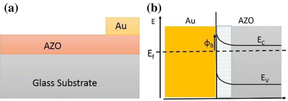
Fig. 1
a
Schematic representation of the metal (Au) electrode fabrication on AZO thin film for electrical contact investigation.
b
Schematic energy band diagram of metal (Au)–semiconductor (AZO) interface without interface states according to Schottky model
The thicknesses of the films were measured by a DEKTAK3 profile meter. X-ray diffraction (XRD) was performed on STOE-XRD diffractometer using Cu-K
α
line (
λ
= 0.15406 nm) in the range of 10–90°. The compositional depth profile was studied by Rutherford backscattering spectrometry (RBS) using a 2.0 MeV He
+
ion beam. The recorded RBS spectra were processed by the SIMNRA simulation computer program [
10
]. The DC electrical conductivity was measured by cooling samples in a continuous He flow in cryogenic units (optical low-temperature model CCS 450 USA) in a thermostatic chamber in the temperature range of 15–520 K. ORTEC (456, USA, 0–3 kV) high-voltage–power supply, Metrix VX102A (FRANCE) and Keithley 196 system DMM (USA) electrometers at a temperature range of 15–500 K were used for voltage and current measurements, accordingly.
Theoretical details
The leakage current of our measurement system was a few microamperes during the temperature-dependent current–voltage measurements. Accordingly, we focused our attention on the temperature-dependent current–voltage measurements under the positive applied voltage regime for extraction of the barrier height. There are several possible conduction mechanisms along with their characteristic temperature dependence and applied voltage dependence of the transport properties such as the current density. One of these mechanisms is the thermionic emission, which has been extensively studied in the context of metal tunnel junctions and semiconductor devices. From the experimental results presented in this work, i.e., the current–voltage characteristic and their temperature dependence, we can simulate the injection of charge carries by the thermionic emission conduction mechanism. In this mechanism, we assume that the current density flows across the barrier and is dependent on the barrier height only [
11
,
12
].
Based on the thermionic emission theory, the equation describing the injection current density across the Schottky contact at the absolute temperature
T
and the applied voltage
Va
is obtained as [
11
,
13
]
Jth=A∗T2exp-φB-ΔφkBT,
where
kB
is the Boltzmann constant,
φB
and
Δφ
are the potential barrier height between the metal and semiconductor and the Schottky barrier lowering, respectively. The lowering of the Schottky potential barrier occurs due to the image charge lowering effect; the relationship between the electrical field and Schottky potential barrier lowering is expressed as:
Δφ=e3E4πεs,
where
e
,
d
and
εs
are the electric charge, the barrier width and the permittivity of the semiconductor, respectively. We may recall
ΦB=φB-Δφ
as the effective Schottky barrier height at zero bias, which is a function of the electric field in the semiconductor through the barrier lowering effect and their surface states. In Eq. (
1
),
A∗=4πem∗kB2h3
is the Richardson constant, which is proportional to the effective mass of electron in the semiconductor (
m∗
) and otherwise contains only the electron charge (
e
) and the Planck’s constant (
h
). The considered conduction mechanism takes place when the effective potential barrier becomes relatively small and the electrons are excited over it. This process is a coherence mechanism and has a temperature dependence and applied voltage dependence. From the viewpoint of thermionic emission theory, the equation describing the temperature-dependent current–voltage measurements [see Eq. (
1
)] can be rewritten in the pass direction across the Schottky contact as:
Jth=A∗T2exp-ΦBkBTexpe(Va-AcJthRs)nkBT-1.
Here,
n
,
Ac
and
Rs
are an ideality factor, the contact area and the series resistance, respectively. From this equation, we can determine the Schottky contact parameters such as the barrier height, the ideality factor and the saturation current. According to this expression, one can conclude that the change of
ln(Jth/T2)
as a function of 1/
T
yields a straight line from which the effective height of the barrier can be calculated from the slope of the line. On the other hand, the applied voltage dependence of the thermionic current density can be calculated via the relation of
ln(Jth)∼Va1/2
at low bias. For the ohmic contacts, the characteristic of electrical property is the specific contact resistance,
ρc,
which is defined as the inverse of the derivative of current density with respect to the voltage evaluated at zero bias, namely
ρc=∂Jth∂VaVa=0-1.
This equation can be also rewritten as
ρc=limAc→0RcAc,
where
Rc
is the total contact resistance.
Results and discussion
Structural and optical analysis
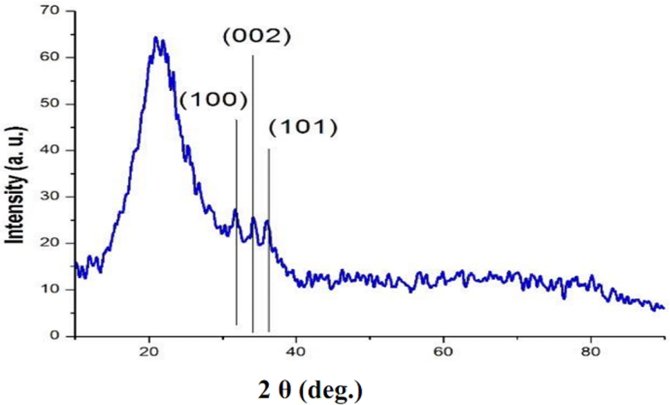
XRD pattern of AZO on glass substrates show three weak peaks appearing at 31.7, 34.0, and 36.0° related to (100), (002) and (101) planes, respectively, of ZnO in its hexagonal structure with a little shift to lower degrees which can be assigned to Al in this structure according to the JPDS card No. [0075-080-01] [
9
,
10
], which indicates the existence of aluminum in the segregation boundaries and increase of the oxygen capture content by the Al
3+
ions compared to Zn
2+
with a larger atomic charge, and the tension or strain resulting from it will cause the (002) plane to move toward the lower degrees [
14
]. To calculate the average size of the crystalline domains of deposited films, we used the Debye–Scherrer equation as follows [
15
,
16
]:
t=0.9λβcosθ,
where
λ
stands for the X-ray wavelength in nm,
β
is the line broadening at half the maximum intensity (FWHM), and
θ
is the angle at which the most intense peak occurred (called also the Bragg angle). The result of XRD spectrum of the ZnO thin film on the Au-coated silicon substrate has been plotted in Fig.
2
.
Fig. 2
XRD spectrum of the electrodeposited ZnO thin film on the Au-coated glass substrate
The main factor of stress in thin films is the difference in thermal expansion between the substrate and the layer. Therefore, the stress is caused by temperature variations in the thin film or substrate due to their different thermal expansions. The strain,
ε
, and the stress,
σ
, in a thin film are calculated according to the following equations [
17
]:
ε=cfilm-cbulkcbulk,σ=-233×109cfilm-cbulkcbulkPa.
Here,
cbulk
and
cfilm
are the lattice constant without strain, in the bulk and layer situation. The parameters extracted from Fig.
2
for the AZO thin film are shown in Table
1
.
Table 1
The extracted details of the XRD analysis from Fig.
2
for the AZO films
Sample
Angle 2θ )o(
Lattice constant (Å)
FWHM (°)
Grain size (nm)
Strain
Stress (× 109 Pa)
AZO
31.75
34.10
c = 5.3
a = 3.26
0.952
0.624
13.4
0.089
− 3.570
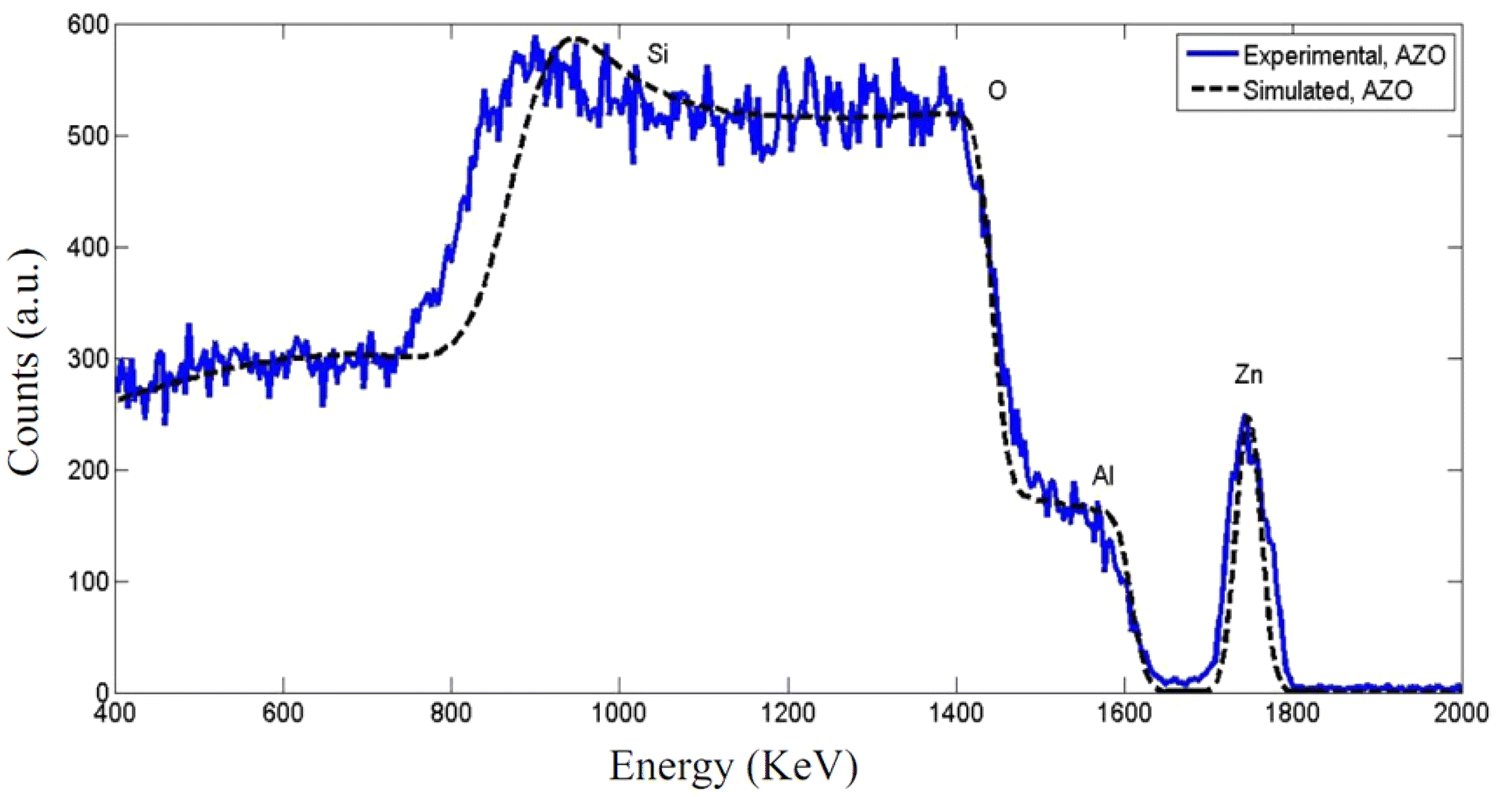
To investigate the structure properties of the AZO thin film, we have studied the Rutherford backscattering spectrometry (RBS) spectrum, which is shown in Fig.
3
. The spectrum determines the contents of elements Zn, Al, and O in the sample. On the other hand, the RBS spectrometry confirms the XRD analysis of AZO thin film for the presence of Al in this thin film.
Fig. 3
RBS analysis of the electrodeposited AZO thin film on the Au-coated silicon substrate
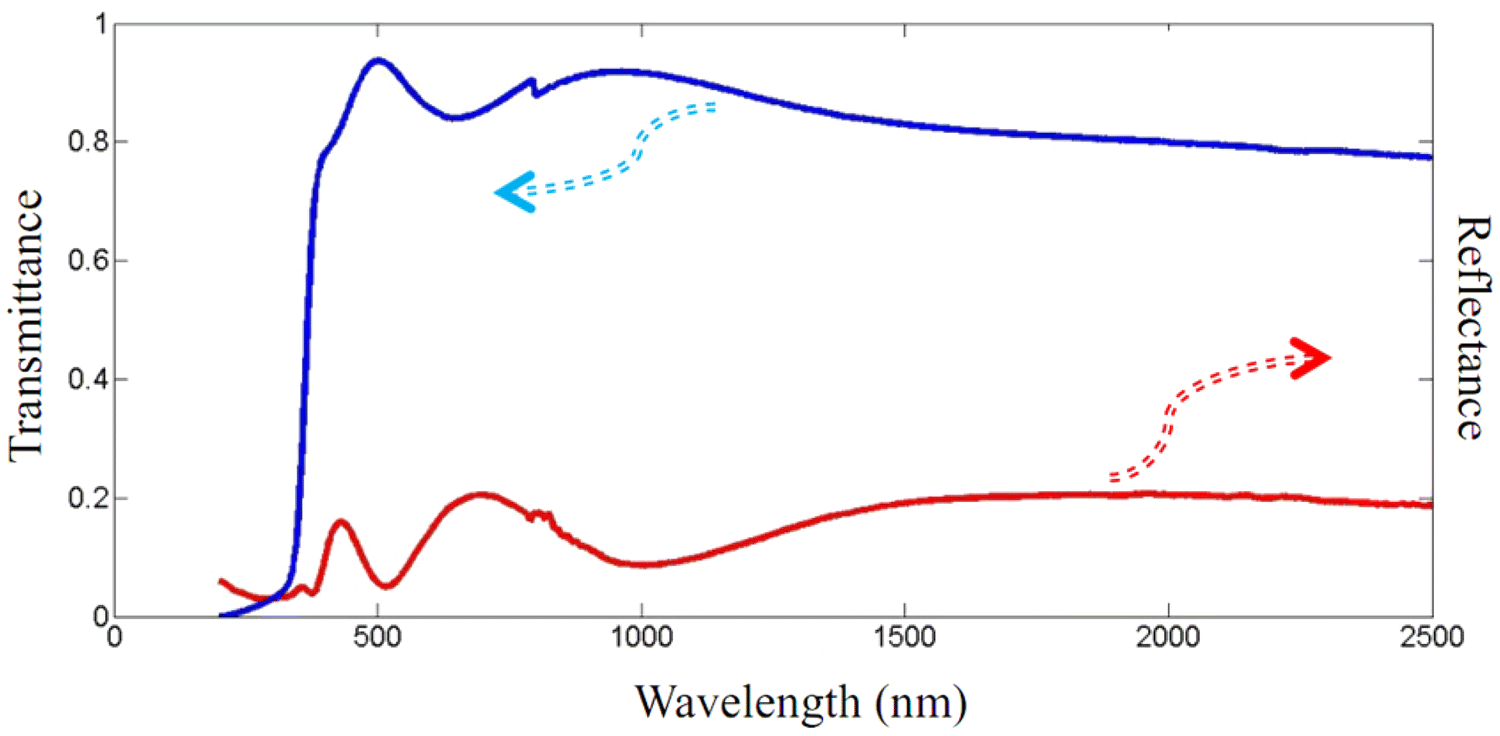
Moreover, we have studied the optical properties of the AZO thin film. For this purpose, the transmittance and reflectance spectra of AZO thin film have been shown in Fig.
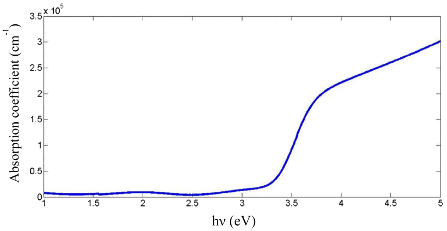
4
. The curves show nearly 90% transmittance in the AZO film, which is a transparent material. Moreover, we have shown the absorption coefficient
α(λ)
of the considered thin film in Fig.
5
. To calculate the absorption coefficient, we have used the following relation [
18
]:
αλ=1dln1Tλ.
Fig. 4
Transmittance (blue curve) and reflectance (red curve) spectra of the electrodeposited AZO thin film on the Au-coated silicon substrate
Fig. 5
Absorption coefficient of AZO thin film
In Eqs. (
1
,
3
),
Tλ
and
d
are the transmittance and film thickness, respectively.
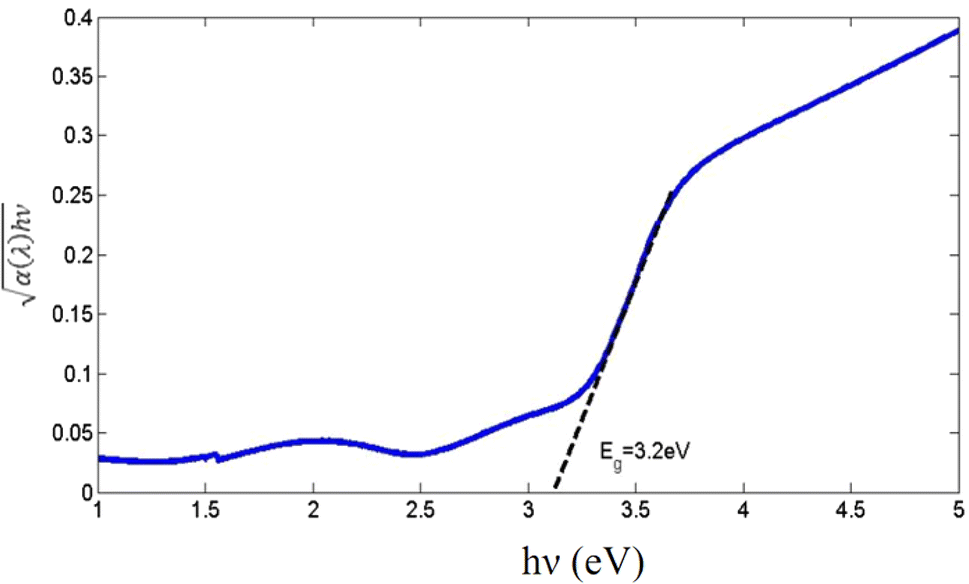
The dependency of absorption coefficient values (
α
) on photon energy determines optical bandgap,
Eg
, via Tauc’s relation [
19
],
αλhν=Ahν-Egm,
where
A
depends on the transition probability. Here,
hν
is the photon energy and
m
is an index of optical absorption characterization process which is theoretically equal to 2 and 1/2 for the allowed indirect and direct transitions, respectively. Figure
6
shows the Tauc’s plot of
αλhν
versus
hν
which results in
Eg
. The bandgap energy (
Eg
) of the AZO thin film, calculated from the
αλhν-hν
characteristics of the devices, yielded value from 3.2 eV, which is similar to values reported in the literature [
15
].
Fig. 6
The curve of
αλhν
as a function of
hν
in the AZO thin film with the thickness of 150 nm. The extracted bandgap energy of the AZO has been obtained as 3.2 eV
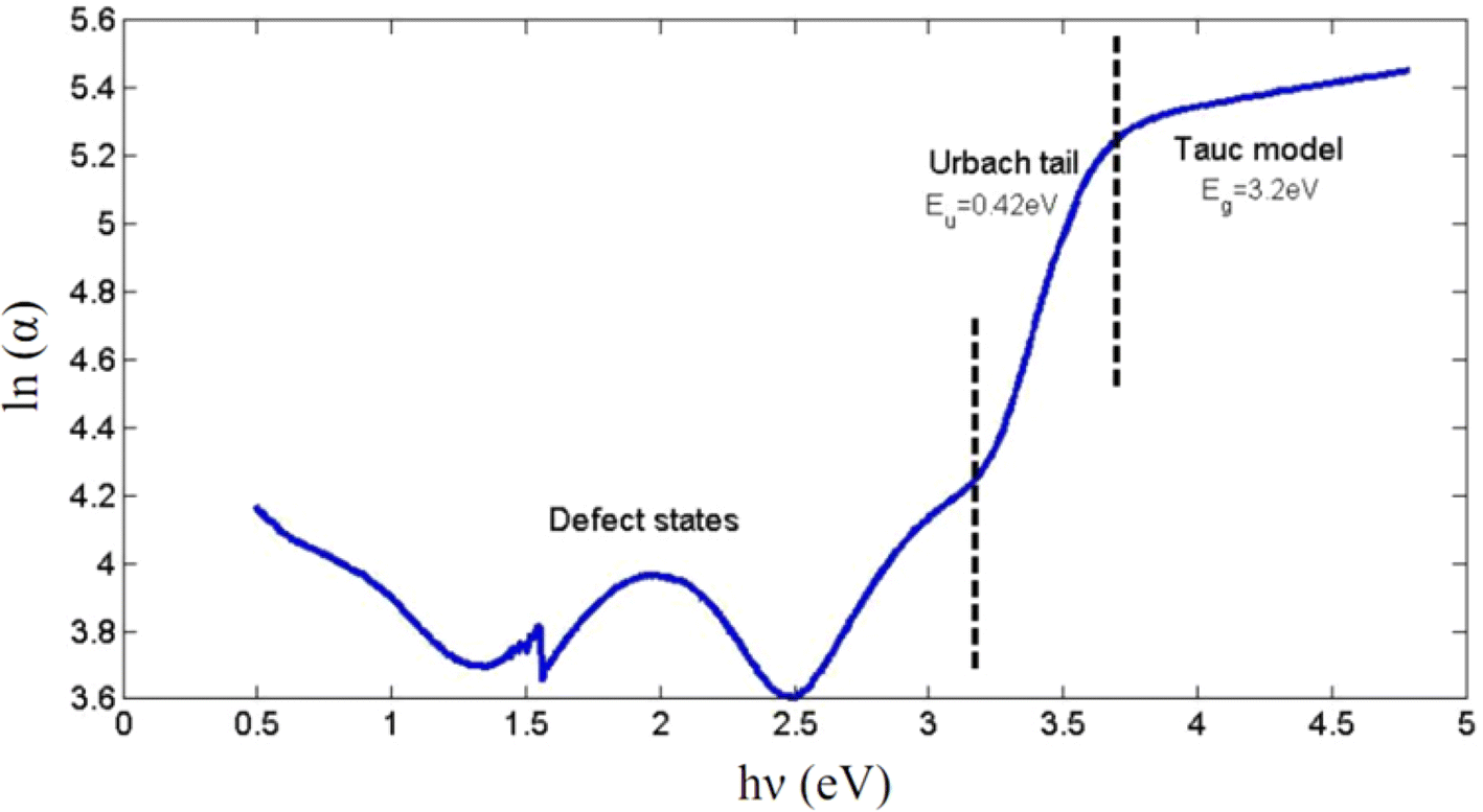
The absorption coefficient at the photon energy below the optical gap (tail absorption) depends exponentially on the photon energy,
αλ∼exphνEu,
where
Eu
is called Urbach energy which is represented in Fig.
7
. The absorption edge, called the Urbach energy, depends on temperature, lattice thermal vibrations, induced disorder, static disorder, strong ionic bonds, and average photon energies [
20
], which were interpreted as the transition between the extended states in one band of the absorption. Log
α
versus
hν
has been plotted in Fig.
7
, which has been resulted in the values of
Eu
= 0.4 eV by least square fitting. The analysis of imperial measurements in nanocontacts helps to understand their functional role in the test surface [
21
].
Fig. 7
The presentation of the function, Ln α as a function of the photon energy,
hν
. This curve can define the Urbach tail, Tauc and defect regions for AZO thin film
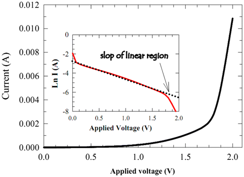
Electrical analysis
In this section, we discuss about the electrical properties of the considered junction, theoretically. For this purpose, at first, the current feature has been plotted as a function of the applied voltage at temperature
T
= 300 K, in Fig.
8
, when
dAZO=150nm
. It is seen that the current varies linearly at low voltage, whereas, with increasing applied voltage, the effective width of the barrier becomes narrower and a nearly parabolic dependence of current on the voltage appears, which indicates the Schottky nature [
22
]. The ohmic behavior of Au/AZO junction is same as In/Zn electrodes on AZO thin film [
23
]. The leakage currents are in order of 0.001 Å. Moreover, we have shown the curve of
ln(I)
as a function of the applied voltage,
Va
in the AZO thin film with the thickness of 150 nm in inset of Fig.
8
. The ideality factor is being measured using the slope of linear region of current–voltage characteristics using the thermionic emission model [Eq. (
1
)] via the relation
n=ekBTdVadln(I)
, [
24
], and its value is obtained as 10.
Fig. 8
Characteristic current–voltage measured from a series of the ZnO thin film samples under Au/AZO configuration revealing a good ohmic contact demonstrating a typical Schottky contact behavior. The inset shows the plot of
ln(I)
vs. the applied voltage, in which the ideality factor is measured using the slope of linear region of current–voltage characteristics
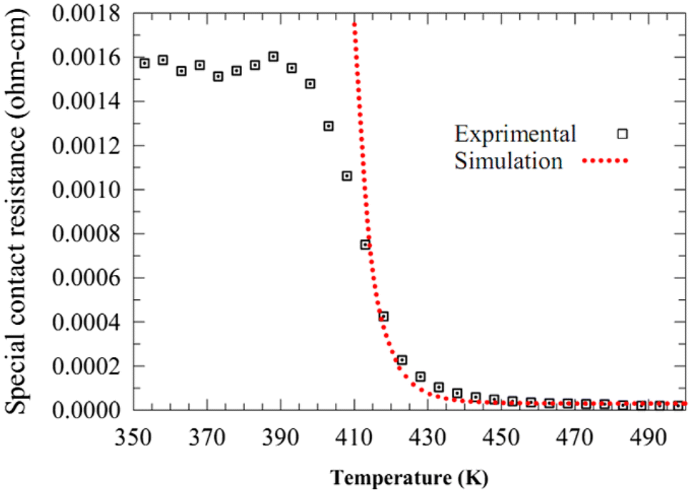
Typical experimental and theoretical special contact resistance characteristics of the Schottky junction are plotted in Fig.
9
. This indicates that the resistivity is composed mainly of tunneling current passing through the Schottky barrier [
11
]. By comparing the experimental and simulation results, the effective barrier height of the Au Schottky barrier yields
ΦB=0.39eV
, which is similar to values reported in Ref. [
25
]. Also, the series resistance,
Rs
, is obtained as 110 Ω. The probability difference of our result with the some other reported on the Au/ZnO interface may be due to the trap of the charge carrier at the substrate during the first stage of the electrodeposition process where some charge carrier could be captured at the interface between Au substrate and the ZnO buffer layer. As it is observed from the figure, the best fit of the experimental and theoretical data is in more than 410 K temperature. The reason is related to the used theoretical model in which current flow mechanism dominates based on the diffusion and thermionic emission currents [
26
]. These currents depend on the density of the available charge carriers in the interface of metal–semiconductor junction and its value is evaluated from the Maxwell–Boltzmann probability distribution function at high temperature. According to the thermionic emission theory, the presented form of temperature dependence of current and also special contact resistance [i.e., Eqs. (
3
) and (
4
)] are compatible at high temperature. While at low temperature, the quantum–mechanical tunneling process through the Schottky barrier between metal–semiconductor junctions dominates, and the current flow mechanism is based on the Fermi–Dirac distribution function.
Fig. 9
Measured special contact resistance characteristic (square symbols) of an Au/AZO junction compared with calculation based on the thermionic emission theory (dotted line)
Conclusions
The AZO thin films were prepared by reactive DC-magnetron sputtering method, in oxygen/argon gases, at 150 nm thickness. XRD pattern of AZO thin film has shown that (100), (002) and (101) planes of ZnO structure had some shifts to lower angles and the RBS analysis has proved the existence of Al in the film. Transmittance spectra have identified the nature of the transparency of AZO film. Optical bandgap and Urbach energy of AZO film are calculated. Also, the electrical behavior of AZO/Au structure and the temperature-dependent resistivity are compared with theoretical result that indicated Au contact at different temperatures exactly complied tunneling current passing through the Schottky barrier. Therefore, we could identify that Au contact is a suitable electrode for thermoelectric devices, gas sensors and dye-sensitized solar cells.
Publisher's Note
Springer Nature remains neutral with regard to jurisdictional claims in published maps and institutional affiliations.
References
Kim et al. (2003) Improved performance of a dye-sensitized solar cell using a TiO2/ZnO/Eosin Y electrode (pp. 495-505) 10.1016/S0927-0248(03)00065-5
Unknown ()
Dejam et al. (2016) Structural and optical characterization of ZnO and AZO thin films: the influence of post-annealing (pp. 685-696)
Dejam et al. (2017) Influence of AZO amorphous structure on n-AZO/p-Cu2O heterojunction diode photoluminescence properties (pp. 9378-9386)
Göde et al. (2011) Influence of annealing temperature on the structural, optical and electrical properties of amorphous zinc sulfide thin films10.1088/1742-6596/326/1/012020
Pathirane et al. (2017) Al-doped ZnO/Ag-nanowire composite electrodes for flexible 3-dimensional nanowire solar cells10.1038/s41598-017-07180-1
Dalouji et al. (2016) Influence of annealing temperature on berthelot-type hopping conduction mechanism in carbon–nickel composite films10.1088/0256-307X/33/5/057203
Ţălu et al. (2015) Characterization of Cu–Ni NPs@a-C: H films by AFM and multifractal analysis (pp. 5662-5670) 10.1021/acs.jpcb.5b00042
Roy et al. (2016) Investigation of nanostructured Pd–Ag/n-ZnO thin film based Schottky junction for methane sensing (pp. 199-210) 10.1007/s40089-016-0187-6
Wang et al. (2013) Mechanism of electron conduction in self assembled alkanethiol monolayer devices10.1103/PhysRevB.68.035416
Schottky (1914) The influence of the structural effects, especially the Thomson graphic quality, on the electron emission of metals (pp. 872-878)
Salam et al. (2013) Sol-gel synthesis of intrinsic and aluminum doped zinc oxide thin films as transparent (pp. 242-247) 10.1016/j.tsf.2012.10.079
Ţălu et al. (2016) Microstructure and micromorphology of ZnO thin films: Case study on Al doping and annealing effects (pp. 109-121) 10.1016/j.spmi.2016.03.003
Cuility (1959) Addison-Wesley, Reading, Mass
Lupan et al. (2010) Effects of annealing on properties of ZnO thin films prepared by electrochemical deposition in chloride medium (pp. 1895-1907) 10.1016/j.apsusc.2009.10.032
Solaymani et al. (2017) Correlation between the multifractal structure, crystalline and photoluminescence properties of engineered CZO thin films (pp. 14205-14219) 10.1016/j.ijhydene.2017.04.045
Tauc et al. (1966) Optical properties and electronic structure of amorphous germanium (pp. 627-637) 10.1002/pssb.19660150224
Sakr et al. (2010) Optical spectroscopy, optical conductivity, dielectric properties and new methods for determining the gap states of CuSe thin films (pp. 557-562) 10.1016/j.jallcom.2010.08.022
Ţăfan et al. (2016) Micromorphology analysis of specific 3-D surface texture of silver chiral nano-flower sculptured structures10.1016/j.jiec.2016.08.003
Ţăfan et al. (2017) Micromorphology investigation of GaAs solar cells: case study on statistical surface roughness parameters10.1007/s10854-017-7422-4
Zhuge et al. (2005) ZnO p–n homojunctions and ohmic contacts to Al–N-co-doped p-type ZnO10.1063/1.2012521
Aydoğan et al. (2009) Electrical characterization of Au/n-ZnO Schottky contacts on n-Si (pp. 913-918) 10.1016/j.jallcom.2008.09.131
Brouri and Leprince-Wang (2014) Schottky junction study for electrodeposited ZnO thin film and nanowires10.1051/epjap/2014140211
Yan et al. (2014) Schottky or ohmic metal–semiconductor contact: influence on photocatalytic efficiency of Ag/ZnO and Pt/ZnO model systems (pp. 101-104) 10.1002/cssc.201300818