Department of Physics, University of Rajshahi, Rajshahi, 6205, BD
Department of Physics, Rajshahi University of Engineering and Technology, Rajshahi, 6204, BD
Abstract
We have investigated the structure, morphology and opto-electric properties of CdO and Ag-incorporated CdO thin films prepared by chemical spray pyrolysis (CSP) method. The X-ray diffraction (GIXRD) study confirms that CdO samples are highly polycrystalline with cubic structure. The AFM study shows smooth surfaces both for CdO and Ag-CdO thin films. The direct band gap energy varies from 2.25 to 2.50 eV depending on Ag content in the films. Urbach energy reversal in optical band gap indicates that several localized states are present above Fermi level or near at the conduction band. The optical properties, such as refractive index, optical conductivity and nonlinear optical susceptibility, are found dependent on Ag content. A combined effect on the transport properties has been observed with the incorporation of Ag in CdO. The metal-like electric conduction of CdO film has been removed up to a temperature T
c
for Ag doping. The n-type carrier concentration of CdO is reduced with increasing Ag content and the concentration is of the order of ~ 10
20
cm
−3
.
Introduction
CdO is a familiar n-type semiconductor with band gap energy (2.2–2.7) eV [
1
,
2
–
3
]. It is transparent to electromagnetic radiation in the visible to NIR spectral regions. The electrical conductivity ranges from ~ 10
2
to ~ 10
4
S/cm. Such a high electrical conduction in CdO is due to Cd interstitials (Cd
i
) and oxygen vacancies (
Vo
) in which (
Vo
) acting as doubly ionized (+ 2) charge donors [
4
]. The CdO-based TCOs draw interest due to relatively simple crystal structures, higher carrier mobility and sometimes nearly metallic conductivities [
5
,
6
]. Although CdO is normally a semiconductor but it shows poor metallic behavior from room temperature (RT) to a certain extent of temperature due to the excess of cadmium atoms in its crystal lattice [
7
]. In general, the opto-electrical properties of undoped and doped CdO films depend on microstructure which can be controlled by changing the preparation conditions. The carrier mobility is one of the key opto-electronic properties which can be controlled by doping CdO with different metallic ions in different deposition techniques [
8
,
9
–
10
]. Among these, spray pyrolysis has some significant advantages over other techniques because of its simplicity, low cost, capability of large area film preparation at air ambient and flexibility of compositional variation to improve expected physical properties.
Previously, we have reported that doped and undoped CdO films prepared by spray pyrolysis technique possess the properties suitable for buffer layer or absorber in solar cells [
11
,
12
], optical switching and photovoltaic applications [
13
,
14
]. Moreover, metallic behavior of CdO was completely removed by Al doping and carrier concentration was increased with increasing Al concentration of spray deposited film [
7
]. The orbital energy of Ag metal is low [
15
] and it has high chemical reactivity in solution among IB group elements. Therefore, to reduce the degeneracy of CdO, Ag can be used to induce semiconducting behavior from RT to elevated temperature. To this end, we have prepared CdO thin films with different concentration of (1, 2, 3 and 4 mol %) Ag, by spray pyrolysis method and studied the effects of Ag on structural and opto-electrical properties of CdO film for opto-electronic applications. The different results obtained in this study are discussed on the basis of existing theories.
Experimental
CdO and Ag-incorporated CdO (Ag-CdO) thin films were deposited on glass substrate by spray pyrolysis technique at 350 °C in an ambient atmosphere. The detail of film preparation and optimization processes for a good quality film has given elsewhere [
7
]. The CdO and Ag-CdO thin films were prepared from aqueous cadmium acetate and silver nitrate solutions. The possible chemical reactions take places on the heated substrate which are as follows:
CdCH3COO2·2H2O+H2O→Decomposes to350∘CCdO+CO2g+CH4g+steamgCdCH3COO2·2H2O+AgNO3·9H2O+H2O→Decomposes to350∘CAg - CdO+NOgCO2g+CH4g+Steamg
The XRD study was performed by X-ray diffractometer (X’-Pert Phillips, Japan). The XRD scan was recorded within Bragg angle 20° ≤ 2
θ
≤ 80° using CuK
α
radiation of wavelength = 1.5405 Å. The surface morphology of CdO and Ag-CdO films was studied by non-contact mode atomic force microscopy using NCHR-tip (AFM-Model: XE70 PARK SYSTEMS). The optical transmission spectra of the film with respect to glass substrate were taken for the wavelength range (380–1000) nm using UV spectrophotometer (UV-1601PC SHIJMADZU SPECTROPHOTOMETER). The Hall-voltage and electrical resistance measurements were performed using the van der Pauw’s method.
Results and discussion
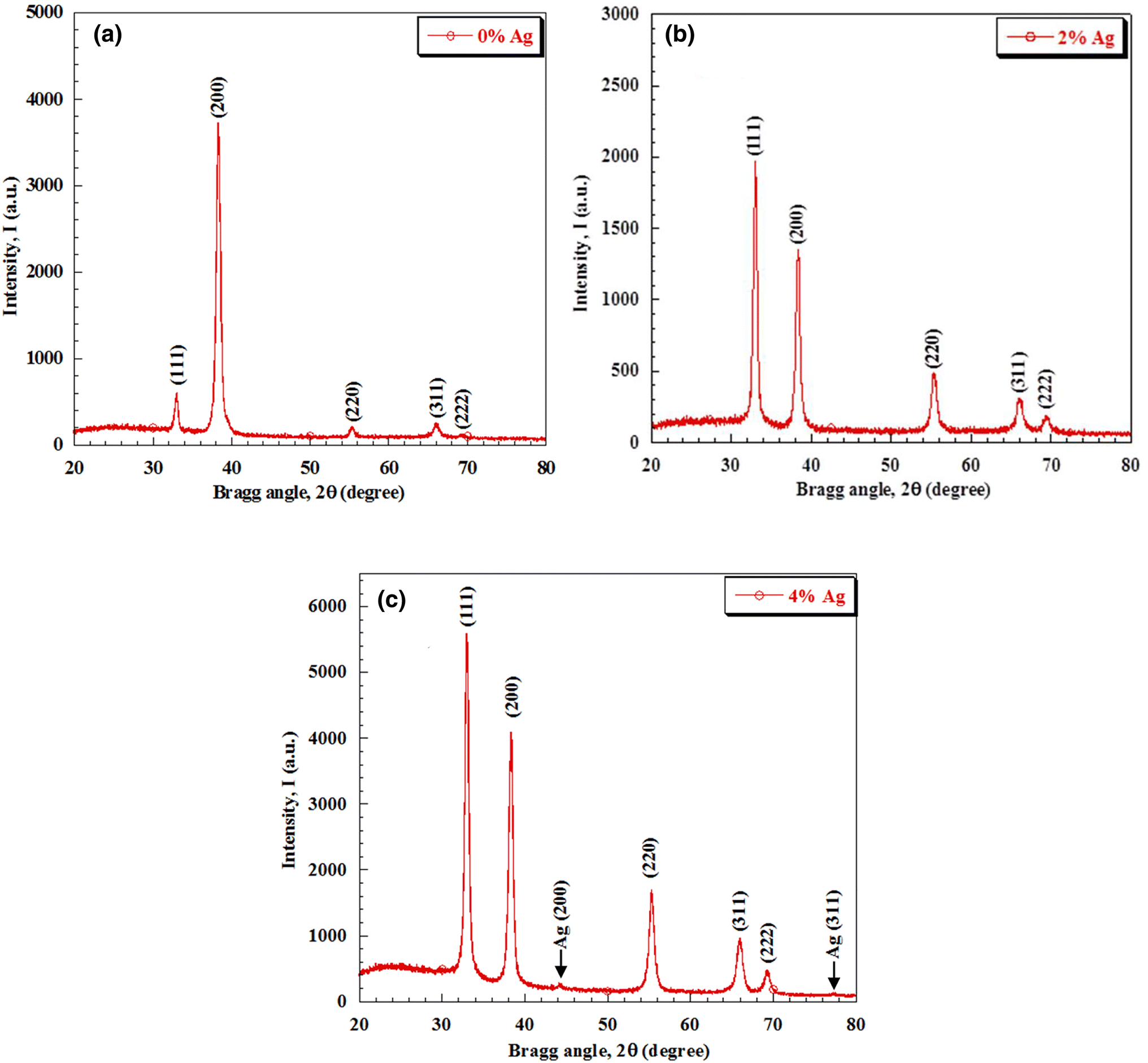
The X-ray diffraction (XRD) patterns for the CdO and Ag-CdO (2 and 4 mol %) thin films are shown in Fig.
1
a–c. The diffraction peaks appeared at 2
θ
° = 33.03°, 38.37°, 55.36°, 66.07° and 69.16° were assigned to the corresponding (
hkl
) values (1 1 1), (2 0 0), (2 2 0), (3 1 1) and (2 2 2), respectively. Two small additional peaks for Ag phase were found at 44.2° and 77.8° for 4 mol % Ag-CdO sample as shown by an arrow in Fig.
1
c, corresponding to the phase observed by Hong-Liang et al. [
16
] in magnetic sputtered samples. The cubic crystal symmetry and preferred orientation in (2 0 0) plane were confirmed by comparing the CdO peaks with standard JCPDS card Nos. 361451 and 732245. Upon Ag doping in CdO, the preferential orientation changed to (1 1 1) plane. Such change in crystallographic orientation by foreign element was reported by Khan et al. [
7
].
Fig. 1
X-ray diffraction patterns of
a
CdO
b
2% Ag-CdO and
c
4% Ag-CdO thin films
The cubic lattice parameter,
a
, estimated from (2 0 0) peak is 0.4687 nm for CdO which is consistent with the reported value 0.4695 nm [
17
]. The lattice parameters for 2 and 4 mol % Ag-CdO are
a
= 0.4694 and 0.4695 nm, respectively. This shows an insignificant change in lattice parameter between CdO and Ag-CdO because of the proximity of their atomic radii (Cd: 1.61 Å and Ag: 1.65 Å), suggesting that Ag may be incorporated at Cd lattice site, vacancy site or at grain boundaries. As a result, there was no significant shifting of peak positions in the XRD patterns.
The crystallite size, ζ, was estimated by Scherer’s formula [
18
]:
ξ=0.94λβcosθ
where
β
is the full width at half maxima (FWHM) expressed in radian. Crystallite size, ζ, was calculated using the FWHM value of major peaks given in Table
1
. It is seen that crystallite sizes are a bit higher for Ag-CdO compared to CdO sample, because the ionic radius of silver is greater than that of cadmium. Moreover, substitution of oxygen vacancies by Ag near the grain boundaries [
19
,
20
] reduces the local strain [
21
] by increasing the crystallite size.
Table 1
XRD peak positions, phase and crystallite size for CdO and Ag-CdO thin films
Sample
(h k l)
Observed 2θ (°)
Standard 2θ (°)
Observed dhkl (Å)
Standard dhkl (Å)
Phase
Crystallite size ζ (nm)
CdO
(1 1 1)
33.03
33.00
2.709
2.712
CdO
23.39
(2 0 0)
38.36
38.28
2.343
2.349
CdO
26.99
2% Ag
(1 1 1)
33.02
33.00
2.710
2.712
CdO
29.25
(2 0 0)
38.36
38.28
2.344
2.349
CdO
24.46
4% Ag
(1 1 1)
33.02
33.00
2.710
2.712
CdO
28.92
(2 0 0)
38.40
38.28
2.342
2.349
CdO
27.15
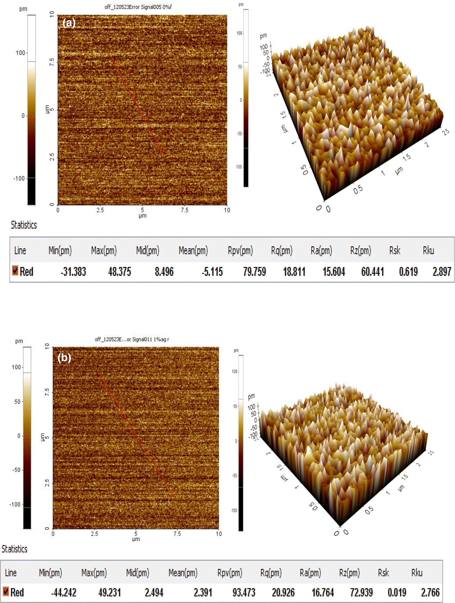
The non-contact mode AFM images for two and three-dimensions are shown in Fig.
2
. The AFM images clearly show that the film surface is very smooth and qualitative because the roughness is very small. The estimated roughness for CdO is 15.604 pm. The roughness for 2 and 4 mol % Ag-CdO samples is 16.764 pm and 19.516 pm, respectively.
Fig. 2
AFM images of
a
CdO,
b
2% Ag-CdO and
c
4% Ag-CdO thin films
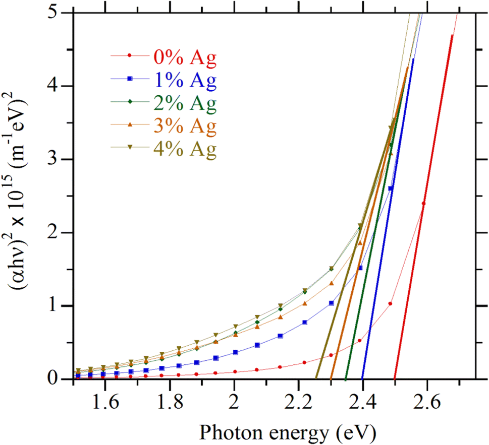
The optical band gap,
Eg
, determined from reflection and transmission data using the classical relation for near band edge optical absorption in a semiconductor is given as:
αhν=Ahν-Eg12
where
α
is the absorption coefficient,
h
is the Plank constant,
ν
is the frequency and
A
is a constant. The linear dependence of
αhν2
on
hυ
at higher photon energies implies that the obtained films are direct transition type semiconductors. The optical band gap,
Eg
estimated from the intercept of the energy axis of Fig.
3
, varies from 2.50 to 2.25 eV, consistent to the reported values of 2.6–2.2 eV for CdO thin films [
2
,
22
]. The band gap narrowing with increasing Ag content in CdO indicates the formation of acceptor energy layer just above the valance band which is influenced by the inverse Burstein-Moss effect [
23
].
Fig. 3
Variation of (
αhυ
)
2
with photon energy for CdO and Ag-CdO thin films
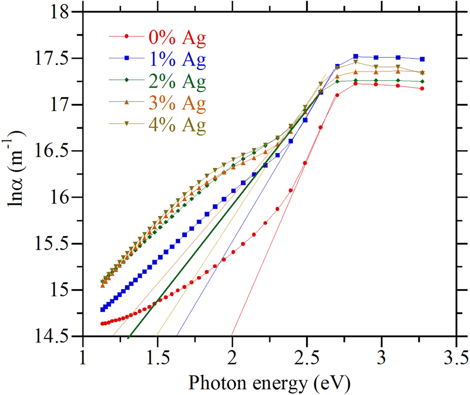
The Urbach tail is an essential parameter used to estimate degree of disorder present in the film materials. Generally, the optical transition and optical band gap structure affected by the width of localized states available in the films which are known as Urbach tail and the Urbach energy
EU
are given as [
24
]:
α=α0exphνEU
where
α0
is a constant. The slope of
lnα
vs.
hν
(Fig.
4
) gives the Urbach energy (0.27–0.51) eV (Table
2
). The band tail width increases from 0.27 to 0.51 eV indicating that the structural disorder increases with increasing Ag doping concentration.
Fig. 4
Dependence of lnα upon the photon energy for CdO and Ag-CdO thin films
Table 2
The values of optical band gap (
Eg
), urbach tail (
EU
), Hall coefficient (
RH
), mobility (
μH
), carrier concentration (
nc
), transition temperature (
Tc
) and activation energy (
∆E
) of CdO and Ag-CdO thin films
Sample
Eg (eV)
EU (eV)
RH ×10-3 (cm3/coul.)
μH (cm2/Vs)
nc × 1020 (cm−3)
Tc (K)
ΔEreversal (eV)
ΔE (eV)
ΔE1
ΔE2
CdO
2.50
0.27
− 12.2
31.69
5.14
374
0.032
− 0.093
0.240
1% Ag
2.40
0.38
− 16.62
33.18
3.76
358
0.031
0.094
− 0.032
2% Ag
2.34
0.46
− 23.55
41.65
2.65
376
0.032
0.061
− 0.029
3% Ag
2.30
0.51
− 27.69
46.05
2.25
380
0.033
0.055
− 0.039
4% Ag
2.25
0.48
− 32.69
52.26
1.91
383
0.033
0.041
− 0.040
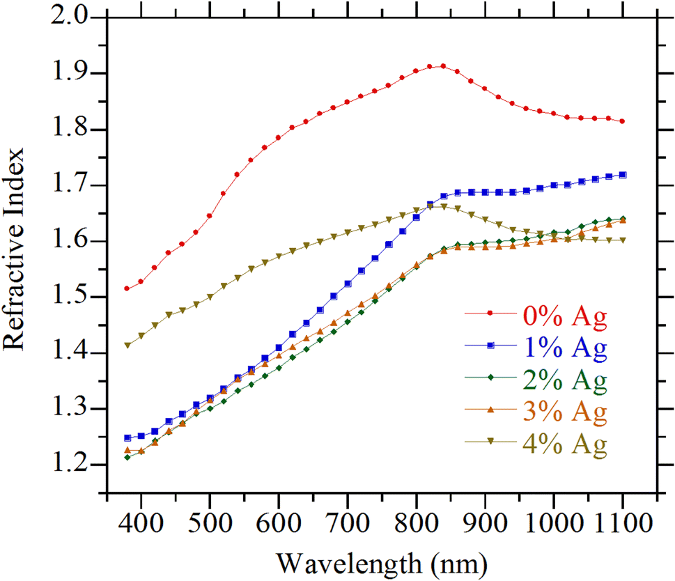
The refractive index (
nr
) of the samples was calculated from the reflection (
R
) and extinction coefficient (
k
) data using the relation [
25
]:
nr=1+R1-R+1+R1-R2-1-k212
The variations of refractive indices with wavelength for different Ag content are shown in Fig.
5
. For CdO, maximum
nr
is 1.90 at 850 nm, while for Ag-CdO thin films,
nr
varies from 1.65 to 1.58. Therefore, it is concluded that
nr
shows anomalous dispersion below 850 nm, followed by normal dispersion after 850 nm. However, the refractive indices of the films show an overall decrease with increasing Ag content due to damping effect and the reduction of reflectance.
Fig. 5
Variation of refractive index with photon energy for CdO and Ag-CdO thin films
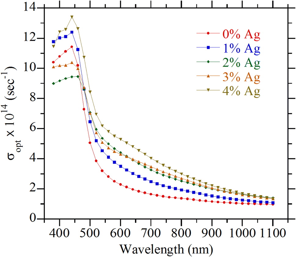
The optical conductivity (
(σopt),
which is a measure of optical response of a material, is given by the relation [
26
]:
σopt=αnrc4π
where
c
is the speed of light. Figure
6
shows the high optical conductivity of the order of 10
14
s
−1
and it increased substantially with increasing Ag concentration. The high value of optical conductivity is due to the increase of electron extinction by photon energy which leads to an increased electronic transfer through the materials [
13
].
Fig. 6
Optical conductivity of CdO and Ag-CdO thin films with wavelength
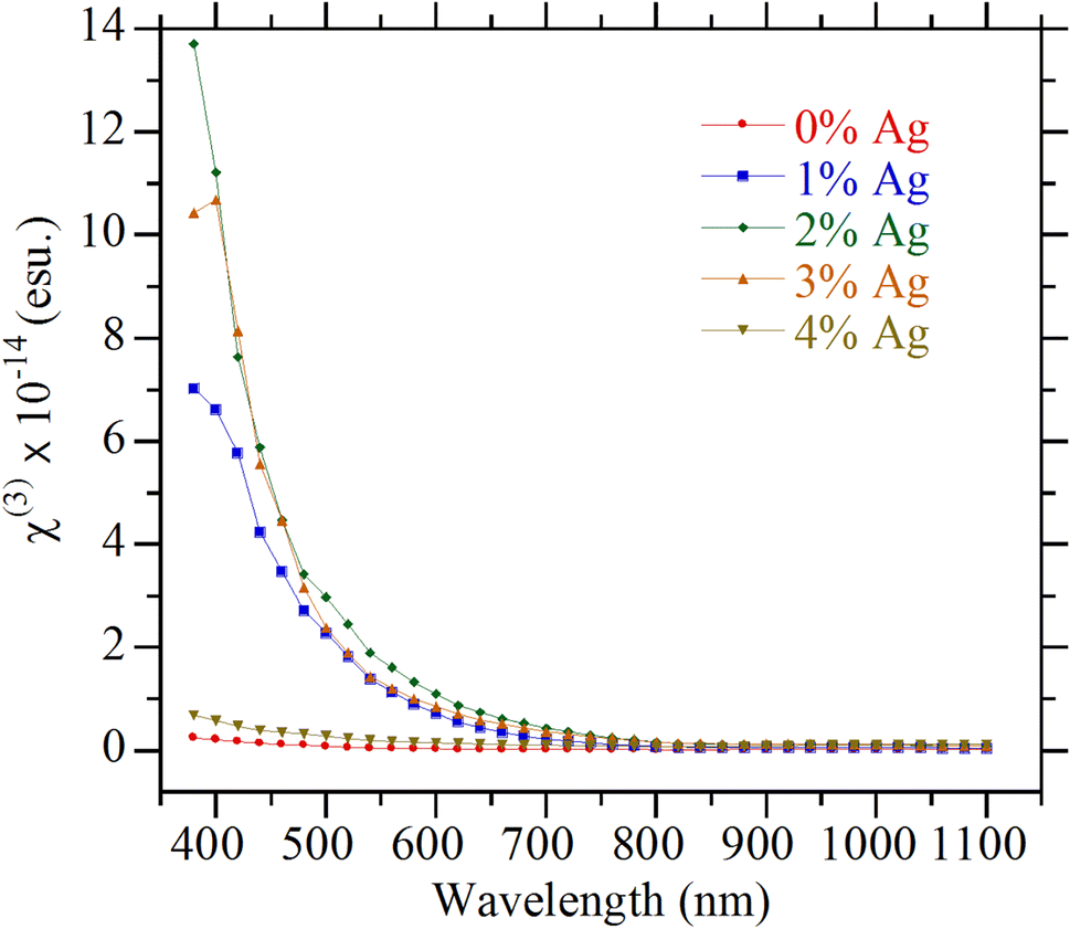
The third-order nonlinear optical susceptibility
χ(3)
, calculated from the refractive index data, is given by the relation [
27
]:
χ(3)=A0(4π)4nr2-14
where
A0
is a constant and equal to 1.7 × 10
−10
esu. Figure
7
shows the variation of
χ(3)
with wavelength as well as Ag concentration. It is clear that the value of
χ(3)
is increased by Ag doping. However, a sharp damping of
χ(3)
in the violet-blue region (< 725 nm) occurred followed by spectral independency. Thus, these samples have the advantage to use as an optical switch.
Fig. 7
Variation of nonlinear optical susceptibility for CdO and Ag-CdO thin films with wavelength
The variation of resistivity with temperature was measured by van der Pauw’s method [
28
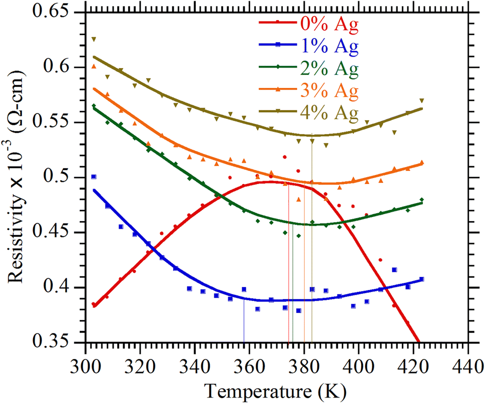
] in the temperature range (303–420 K). Figure
8
shows that the resistivity is dependent on the temperature with increasing Ag content in CdO. The room temperature resistivity for CdO is 0.39 × 10
−3
O-cm which increases with doping and reached 0.63 × 10
−3
O cm for 4 mol % Ag doping. Moreover, the metallic behavior of CdO thin film was washed out due to Ag incorporation. It is also perceptible that two types of conduction mechanism are present for CdO and Ag-incorporated thin films. The resistivity of CdO film increased with increasing temperature up to a certain temperature (
Tc
) 374 K (metal-like) after which resistivity falls up to the measured temperature range as a normal semiconductor. This type of resistivity variation with temperature may be caused due to carrier scattering. However, higher RT resistivity of Ag-incorporated samples compared to CdO could be explained by the electronic configuration of Ag (47) and Cd (48). Since silver (Ag) atom has only one electron in 5 s orbital (4d
10
5 s
1
) and cadmium (Cd) atom has two electrons in 5 s orbital (4d
10
5 s
2
); therefore, when Ag sits at Cd site in CdO matrix a free hole is produced and compensates the electrons of n-type CdO. Subsequently, the electron charge density of doped CdO decreased and this leads to an increase in resistivity at RT.
Fig. 8
Temperature-dependent resistivity for CdO and Ag-CdO thin films
On the other hand, the resistivity of the Ag-incorporated samples decrease from RT to
Tc
like usual semiconductor and then increases with temperature like metal. So the metallic behavior of CdO film was removed completely up to
Tc
with the incorporation of Ag. However, the slight increase in resistivity after
Tc
seems due to scattering caused by thermal agitation of carriers.
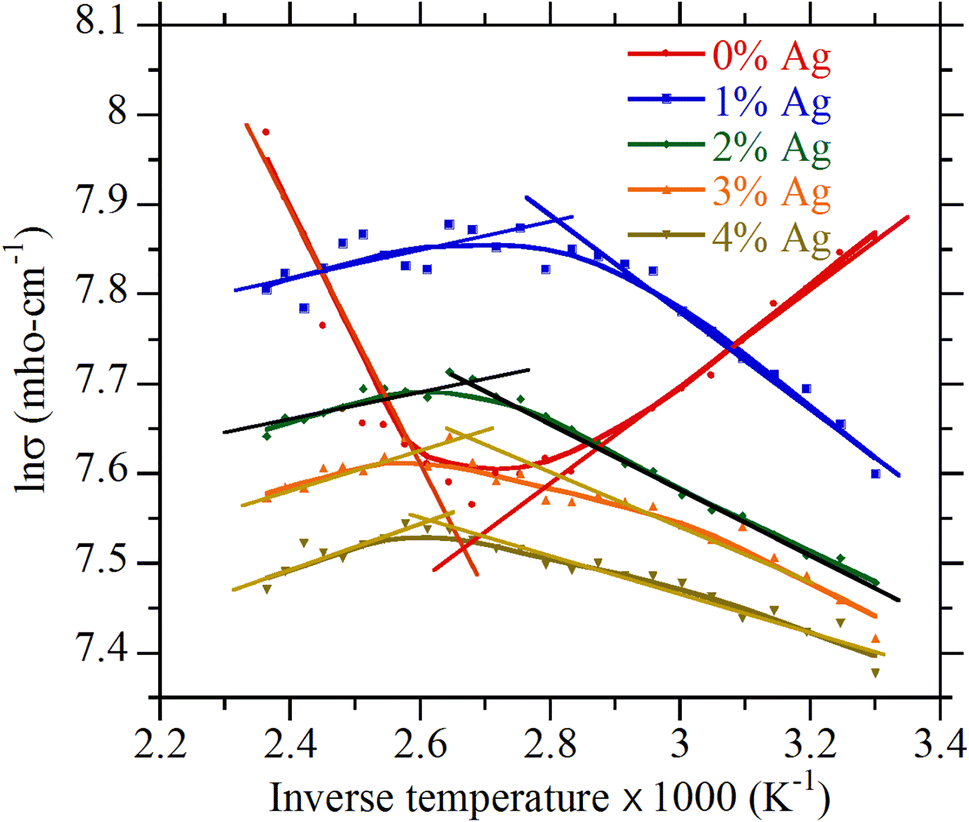
The activation energy was calculated by the relation:
σ=σ0exp-ΔE2KBT
where
ΔE
is the activation energy,
KB
is the Boltzmann constant,
σ
is the conductivity of the film and
σ0
is the pre-exponential factor. Figure
9
shows the variation of lnσ with 1000/T for CdO and Ag-CdO thin films and the slop of the curve gives activation energy. Estimated activation energy
ΔE1
for the low-temperature region (RT to
Tc
) and
ΔE2
for the high-temperature region (
Tc
to measured temperature range) are given in Table
2
. The activation energy reversal defined as
ΔEreversal
=
KBTc
, at which mode of transport phenomenon changes is also given in Table
2
. In low-temperature region,
ΔE1
varies from -0.093 eV to 0.041 eV due to the excitations of carriers from one defect state to another and at high-temperature region,
ΔE2
is lower than
ΔE1
and varies from 0.24 to − 0.040 eV, indicating that conductivity in this temperature region is associated with the free band transition of carriers from donor level to conduction band.
Fig. 9
Variation of lnσ with inverse temperature for CdO and Ag-CdO thin films
Hall voltage measurement was done at a magnetic field of 9.815 kilo-gauss from which Hall constant (
RH
), carrier concentration (
nc
) and Hall mobility (
μH
) have been determined (Table
2
). From the table, it is seen that
RH
is negative and negativity increased with the increase of Ag concentration. Also, the mobility of carriers increases, whereas
nc
decreases with the increase of Ag content. The negative sign of
RH
indicates that the carriers are n-type with the concentration of the order of ~ 10
20
cm
−3
. The reduced carrier concentration originated from the hybridization between Ag-4d and O-2p levels creating a hole when Ag atom substitutes Cd in the crystal lattice.
Conclusion
In the present work, CdO and Ag-CdO thin films were prepared by chemical spray pyrolysis method on glass substrate at substrate temperature 350 °C and structural, optical and electrical properties were investigated. XRD study confirms that CdO and Ag-CdO thin films are polycrystalline with cubic crystal structure. The preferred crystallographic orientation of CdO is in (2 0 0) plane which changes to (1 1 1) as an effect of Ag incorporation. The AFM study confirms that films are very smooth. The direct band gap energy decreases from 2.50 eV to 2.25 eV with increasing Ag concentration which ascertained the inverse Burstein–Moss effect. The value of Urbach energy varies from 0.27 to 0.51 eV and the refractive indices decrease from 1.90 to 1.58 with increasing Ag content. Optical response of the films is found reasonably well. The metal-like behavior of CdO thin film was removed by incorporation of Ag. The activation energy was calculated in two different temperature regions:
ΔE1
varies from − 0.093 to 0.041 eV and
ΔE2
varies from 0.240 to − 0.040 eV. Hall study confirms that all samples are n-type semiconductors having carrier concentration of the order of ~ 10
20
cm
−3
.
Acknowledgements
The authors are thankful to the Bangladesh Council of Scientific and Industrial Research (BCSIR), Bangladesh for providing XRD facility.
Publisher's Note
Springer Nature remains neutral with regard to jurisdictional claims in published maps and institutional affiliations.
References
Zhao et al. (2002) Electrical and optical properties of tin-doped CdO films deposited by atmospheric metal organic chemical vapor deposition (pp. 203-211) 10.1016/S0040-6090(02)00344-9
Dhakel (2008) Influence of hydrogenation on the electrical and optical properties of CdO thin films10.1088/0268-1242/23/5/055017
Dhakel (2015) Development of electrical conduction with beryllium doping of CdO nanostructure thin films (pp. 222-227) 10.1590/1516-1439.301014
Burbano et al. (2011) Sources of conductivity and doping limits in CdO from hybrid density functional theory (pp. 15065-15072) 10.1021/ja204639y
Kammler et al. (2001) Comparison of thin film and bulk forms of the transparent conducting oxide solution Cd1+xIn2-2xSnxO410.1063/1.1410882
Mason et al. (2002) Defect chemistry and physical properties of transparent conducting oxides in the CdO–In2O3–SnO2 system (pp. 106-114) 10.1016/S0040-6090(02)00197-9
Khan et al. (2010) Effect of Al-doping on optical and electrical properties of spray pyrolytic nano-crystalline CdO thin films 10(3) (pp. 790-796) 10.1016/j.cap.2009.09.016
Dou et al. (1998) N-type doping in CdO ceramics: a study by EELS and photoemission spectroscopy 398(1-2) (pp. 241-258) 10.1016/S0039-6028(98)80028-9
Dakhel (2008) Effect of thallium doping on the electrical and optical properties of CdO thin films (pp. 2704-2710) 10.1002/pssa.200723472
Gupta et al. (2009) Preparation and characterization of highly conducting and transparent Al doped CdO thin films by pulsed laser deposition (pp. 673-677) 10.1016/j.cap.2008.06.004
Karim et al. (2015) Structural and opto-electrical properties of pyrolized ZnO—CdO crystalline thin films 36(5) 10.1088/1674-4926/36/5/053001
Karim et al. (2015) Study of the morphology, photoluminescence and photoconductivity of ZnO–CdO nanocrystals 2(3) 10.1088/2053-1591/2/3/036402
Karim et al. (2016) Effect of Zn/Cd ratio on the optical constants and photoconductive gain of ZnO–CdO crystalline thin films (pp. 184-192) 10.1016/j.mssp.2015.08.037
Ashaduzzman et al. (2018) Influence of chromium on structural, non-linear optical constants and transport properties of CdO thin films (pp. 135-144) 10.1016/j.surfin.2018.05.008
Yan et al. (2006) Doping of ZnO by group-Ib elements10.1063/1.2378404
Hong-Liang et al. (2010) Study on the crystalline structure and the thermal stability of silver-oxide films deposited by using direct-current reactive magnetron sputtering methods (pp. 1176-1179) 10.3938/jkps.56.1176
Jarzebski (1973) Pergamon Press
Cullity and Stock (2001) Prentice Hall
McKenna and Shluger (2009) The interaction of oxygen vacancies with grain boundaries in monoclinic HfO210.1063/1.3271184
Joakim et al. (2012) Oxygen vacancy segregation and space-charge effects in grain boundaries of dry and hydrated BaZrO310.1063/1.3681169
Klie et al. (2005) Enhanced current transport at grain boundaries in high-Tc superconductors10.1038/nature03644
Dhakel and Hamad (2012) Investigation on high carrier mobility in chromium incorporated CdO thin films on glass (pp. 25-33)
Flores-Mendoza et al. (2013) Photoluminescence in undoped (CdO)1−x(InO3/2)x thin films at room temperature, 0 ≤ x ≤ 1 (pp. 133-138) 10.1016/j.jlumin.2012.10.030
Urbach (1953) The long-wavelength edge of photographic sensitivity and of the electronic absorption of solids10.1103/PhysRev.92.1324
Abeles (1972) North-Holland
Pankove (1975) Dover Publications Inc.
Mahmoud and Al-Ghamdi (2010) Synthesis of CdZnO thin film as a potential candidate for optical switches (pp. 1134-1138) 10.1016/j.optlastec.2010.02.009
Van-der-Pauw (1958) A method of measuring the resistivity and Hall coefficient on lamellae of arbitrary shape (pp. 220-224)