Department of Electrical Engineering, Rasht Branch, Islamic Azad University, Rasht, IR
Abstract
In this paper, a gallium antimonide junctionless tunnel field-effect transistor based on electrically doped concept (GaSb–EDTFET) is studied and simulated. The performance of the device is analyzed based on the energy band diagram and electric field profile. The on-current, transconductance, and cut-off frequency are enhanced in case of GaSb–EDTFET compared with Si-EDTFET due to the combination of the high tunneling efficiency of the narrow bandgap and the high-electron mobility of GaSb. On the other hand, the Gaussian-doping profile decreases the ambipolar and off current by increasing the tunneling barrier length at the drain/channel interface. Hence, applying Gaussian-doping profile on GaSb–EDTFET makes it a suitable candidate for analog and digital applications. Next, heterostructure channel/source interface EDTFET is studied which uses GaSb for the source and AlGaSb for the drain and channel regions. Then, it has been optimized by numerical simulation in terms of aluminum (Al) composition. The optimal Al composition was founded to be around 10% (
x
= 0.1). It is shown that the blend of Gaussian-doping profile and the heterostructure channel/source interface with optimal Al composition remarkably reduces ambipolar current amount to a value of 1.3 × 10
−23
A/μm. The improvements in terms of
Ioff
,
Ion
,
Ion
/
Ioff
rate, subthreshold swing, transconductance, cut-off frequency, and also suppressed ambipolar behavior are illustrated by numerical simulations.
Introduction
In recent years, the scaling of conventional CMOS transistors and supply voltage have been faced with problems such as high off-state current, SCEs, DIBL, and subthreshold swing limits of 60 mV/dec at room temperature [
1
,
2
–
3
]. Therefore, some various device structures such as double gate [
4
], tri-gate [
5
], gate-all-around (GAA) MOSFET [
6
], and junctionless field-effect transistor JLFET [
7
] have been reported. JLFET has been fabricated without using PN junctions at the lateral junctions. Although it simplifies the fabrication process, it also suffers from the high off-state current. Tunneling field-effect transistors (TFETs) recently replaced the conventional MOSFET due to its steeper subthreshold swing (SS) (< 60 mV/dec) and low off-state current (
Ioff
) which leads to the low values of power consumption [
8
,
9
,
10
,
11
–
12
]. The achievement was obtained due to the band-to-band tunneling (BTBT) carriers rather than drift–diffusion over the barrier. One of the drawbacks of the performance of TFETs is the inferior on-state current (
Ion
) because of the insufficient quantum BTBT limited by the large bandgap of silicon. Hence, it can be solved using low bandgap semiconductors [
13
]. Lately, different methods of improving the performance of TFETs have been presented such as gate engineering [
14
], using heterostructures and high-
k
dielectric [
15
]. TFETs also suffer from ambipolar behavior [
16
,
17
], which is concluded from the presence of symmetric areas of P
+
and N
+
in the source and the drain, the overlapping between the valence band of the channel, and the conduction band of the drain under negative gate bias. In this condition, the channel is accumulated by holes due to BTBT at drain/channel interface. Therefore, it has created a high current drive at the negative voltage similar to the positive voltage. To overcome the ambipolar behavior, researchers have used hetero-gate dielectrics, gate workfunction engineering, asymmetric doping for source and drain [
18
], Gaussian-doping profiles, and gate–drain overlapping [
14
,
16
,
17
,
19
–
22
].
Another drawback in the down-scaling process of TFETs is to fabricate metallurgical junctions due to the need for the creation of abrupt junctions at high temperatures which is difficult and expensive [
7
]. This problem can be solved using junctionless TFETs (JLTFETs) [
22
,
23
]. JLTFET uses high-doping concentrations in the drain, channel, and source. It has provided N
+
–I–P
+
for N-JLTFETs similar to doping profile of an N-TFET using two methods. One method is the use of the charge plasma concept, wherein the desired doping profile is created by choosing appropriate workfunctions for the gates called the polarity gate (PG) located at the source region and the control gate (CG) located at the middle with a lower workfunction than PG for being a nearly intrinsic channel [
24
,
25
,
26
–
27
]. As the same way, p-channel JLTFET has the similar structure [
28
]. Another method to create N
+
–I–P
+
in JLTFET is using the electrically doped concept, in which P
+
region underneath PG is created by applying an appropriate external bias voltage. These devices are known as EDTFET [
29
,
30
–
31
]. The other type of JLTFETs known as dopingless TFETs suppresses the need of a higher thermal budget and expensive thermal annealing technique due to refusing the physical doping [
32
,
33
,
34
,
35
–
36
]. In this structure, the drain region is also gated for creating N
+
using charge plasma or electrically doped concepts. JLTFETs also include inferior
Ion
and ambipolar behavior. To overcome these problems, different methods have been investigated, such as: using heterostructures at source/channel interfaces [
37
,
38
,
39
,
40
–
41
], the assumption of gate workfunction engineering [
42
,
43
,
44
–
45
], the adoption of hetero-gate dielectrics [
46
,
47
,
48
–
49
], using Gaussian-doping profiles [
22
,
50
,
51
], applying source pockets [
52
], the consideration of strain engineering [
53
,
54
], using ferroelectric insulators [
40
], and drain workfunction engineering for DLTFET [
55
,
56
].
The rest of this paper is structured as follows. In Sect.
2
, device simulations and structures are discussed. In Sect.
3
, the DC characteristics for the GaSb–EDTFET are presented which clarify its improvements in analog applications over a basic Si-EDTFET. In Sect.
4
, Gaussian-doping distribution is proposed to decrease the ambipolar current. Section
5
is dedicated to the analysis and calculation of analog parameters, cut-off frequency, and transconductance for the GD–GaSb–EDTFET. In Sect.
6
, heterostructure channel/source interface EDTFET is studied which applies Al
x
Ga
1−
x
Sb for the channel and drain regions and GaSb for the source region (AlGaSb–GaSb–EDTFET). With respect to the Al fraction (
x
), the bandgap energy of Al
x
Ga
1-x
Sb and, consequently, the tunneling probability and the device current vary. Thus, the optimal Al composition is extracted in AlGaSb based on the improving ambipolar current, off-current, on-current, on-to-off current ratio, threshold voltage, and subthreshold swing. Then, it is presented a performance comparison between the structures in DC parameters is presented. Section
7
concludes this paper.
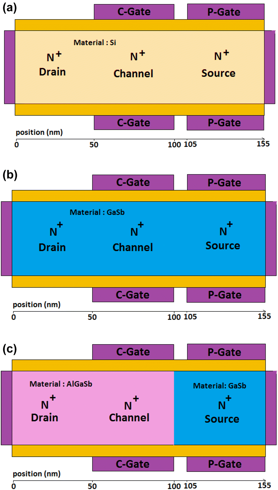
Device structure and simulation
A cross-sectional view of conventional Si-EDTFET is shown in Fig.
1
a, GD–GaSb–EDTFET in Fig.
1
b and GD–AlGaSb–GaSb−EDTFET in Fig.
1
c. A III–V semiconductor has been used in the GD–GaSb–EDTFET, which has a narrow bandgap (0.72 eV) and high carrier mobility [
57
,
58
]. In the GD–AlGaSb–GaSb–EDTFET device, GaSb is used at the source side and AlGaSb at the drain and the channel sides to improve the device performance. It is considered that the channel, source, and drain are heavily n-type doped (1 × 10
19
cm
−3
) in the case of the conventional EDTFET. For the proposed devices (GD–GaSb–EDTFET and GD–AlGaSb–GaSb–EDTFET), Gaussian-doping profile is allocated to channel and drain, although source is kept the uniform doping. All devices consist of two isolated gates (CG and PG) with the same workfunction equal to 4.7 eV. The polarity gate bias voltage VPG = − 1.2 V has been considered for obtaining the desired carriers concentration in the source region. It also provides a concentration gradient at the source/channel interface [
30
,
31
]. In addition, the spacer length (Lgap) is kept 5 nm for creating N
+
-doped pocket layer near to the source. The doping profile of N
+
–I–N
+
–P
+
TFET is formed by electrical doped concept rather than physical doping. High-
k
dielectric was also used to improve the subthreshold swing and on-state current [
15
]. The rest of the device design parameters used in the simulations are listed in Table
1
.
Fig. 1
Device schematic of
a
conventional Si-EDTFET.
b
GD–GaSb–EDTFET,
c
GD–Al
0.1
GaSb–GaSb–EDTFET
Table 1
Device design parameters used in simulation
Parameter
Value
Unit
Gate length (Lch)
50
nm
Equivalent oxide thickness (EOT)
1
nm
Spacer length between CG and PG (Lgap)
5
nm
Silicon thickness (Tsi)
10
nm
Polarity gate (PG)
− 1.2
V
Dielectric constant (hfo2)
25
–
All the electrical characteristics were obtained from 2D ATLAS device simulator [
59
]. A nonlocal BTBT model to calculate band-to-band tunneling of charge carriers between source and channel was included. In this model, the spatial variation of energy bands is taken into account and also the recombination–generation rate at each location is considered based on the electric field to model the tunneling process. The Shockley–Read–Hall model was also used to incorporate the minority recombination due to the presence of high-impurity concentration in the channel and the interface trap effect. It takes into consideration the phonon transitions that occur in the presence of defects or traps within the forbidden gap of the semiconductor. Fermi–Dirac statistics was invoked to calculate the intrinsic carrier concentration required in the expressions for SRH recombination. Auger recombination is a non-radiative process involving three carriers. It occurs when an electron and hole recombine, but instead of producing light, either an electron is raised higher into the conduction band or a hole is pushed deeper into the valence band. Auger recombination is significant in non-equilibrium conditions when the carrier density is very high. To consider this effect, auger recombination model was included. High doping often leads to narrowing of bandgap and is essential to consider especially within the devices which are based on tunneling mechanism. Therefore, bandgap narrowing model is also incorporated. The quantum confinement model was activated to consider quantum confinement effects on BTBT.
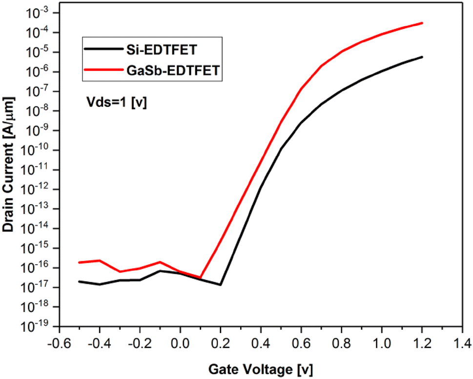
DC-performance analysis
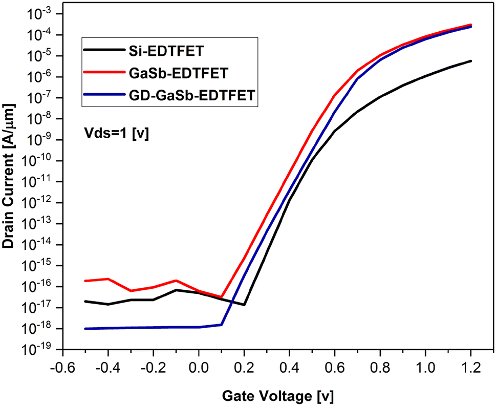
In this section, The DC performance and the comparison of Si and GaSb based on electrically doped concept have been analyzed. Tunneling devices have transported the phenomena entirely different from bulk MOSFET devices. Drive current in TFETs is computed based on band-to-band tunneling from the valence band of source to the conduction band of channel. Electron/hole tunneling probability in this research is calculated using the nonlocal BTBT model on the basis of the Wentzele–Kramere–Brillouin method. Band-to-band tunneling probability strongly depends on material/device parameters such as the screening tunneling barrier length (Λ), energy bandgap (Eg), band energy difference between the valence and conduction bands of tunneling regions (ΔΦ), and effective mass of charge carriers (
m∗
), according to Eq. (
1
) [
3
,
60
–
62
], wherein h and q are the Planck constant and electron charge, respectively:
TE≈exp-4ΛEg3/22m∗3qhEg+Δ∅.
Tunneling barrier length (Λ) given by Eq. (
2
) is sensitive to the dielectric thickness (
tox
), semiconductor channel thickness (
tSi
), dielectric constant of the gate material, and semiconductor (
εSi
,
εox
):
Λ=εsitsitox/εox.
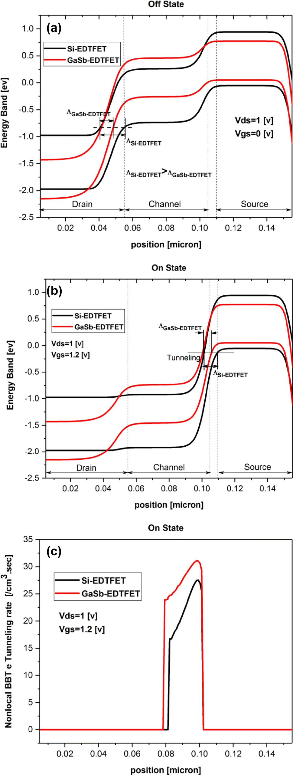
In the N-TFET device, drain is always biased with positive voltage to allow the connections between source–channel and the drain–channel will be in reverse bias. Device current is proportional to tunneling probability, which itself depends on the variation of band structure at the source/channel and drain/channel interfaces. The band structure is changed by varying gate and drain voltages. By overlapping the conduction band with the valence band, tunneling probability is increased at regions. At on state, under the positive gate voltage, an overlap occurs between the conduction band of the channel and the valence band of the source. According to Eq. (
1
), to increase on-state current of EDTFETs, lower bandgap material can be used. In Fig.
2
, it is observed that the on-state current in case of GaSb–EDTFET is higher due to the presence of lower bandgap (0.72 V) of gallium antimonide. At the ambipolar state, in which negative gate voltage is applied, an overlap is created between the conduction band of the drain and the valence band of the channel. Therefore, the ambipolar current is also increased in case of GaSb–EDTFET by applying lower bandgap material. Increasing current is explainable based on the energy band diagram. In Fig.
3
a, b, it can be observed that the tunneling barrier length is narrow at the drain/channel interface (at off state) and is also thin at the source/channel interface (at on state) in case of GaSb–EDTFET. The electron-tunneling rate can also represent the increasing current. Figure
3
c shows the higher electron-tunneling rate for GaSb–EDTFET at on state. The current is also proportional to the electron-tunneling rate, which depends on the transmission probability, according to Eq. (
1
). Therefore, the on-state current significantly increases due to the improving tunneling rate.
Fig. 2
Comparison of conventional Si-EDTFET and GaSb–EDTFET transfer characteristic at Vds = 1.0 V
Fig. 3
Comparison of conventional Si-EDTFET and GaSb–EDTFET.
a
Energy band diagram at the off state.
b
Energy band diagram at the on state.
c
Nonlocal band-to-band tunneling rate at the off state
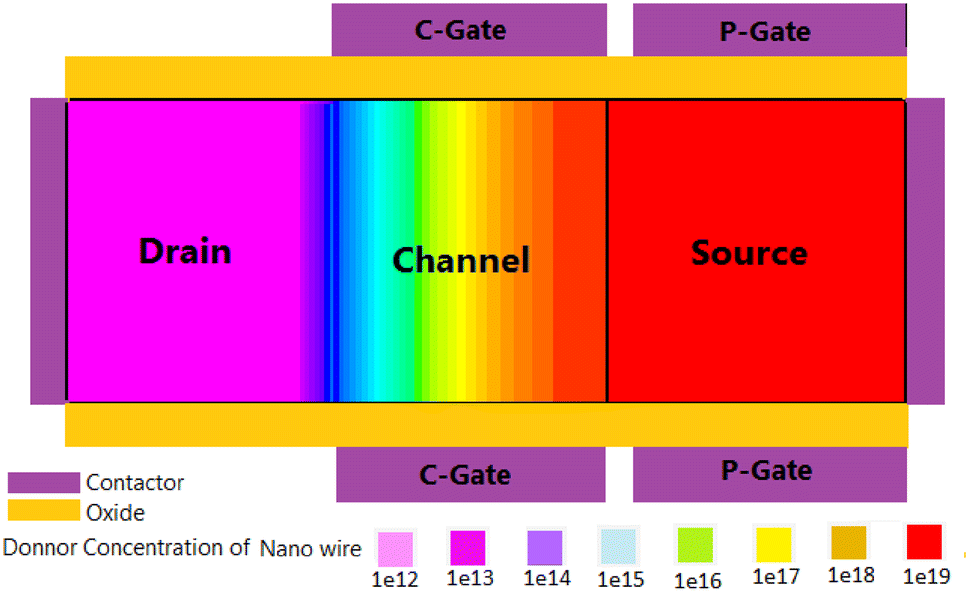
Gaussian-doping profile
To reduce off and ambipolar current, the tunneling barrier length at the drain/channel interface must be increased at off and ambipolar states, which can be achieved by applying the Gaussian-doping profile [
51
]. Based on the results obtained from Sect.
3
, the GaSb–EDTFET has higher on-current than the Si-EDTFET. To improve the performance of the GaSb–EDTFET in digital applications, in addition to analog applications, along with increasing the on-current, reducing the off and ambipolar current is considered. Therefore, in this section, the impact of the Gaussian-doping profile on the performance of the GaSb–EDTFET is studied by applying it in the drain and channel. Figure
4
illustrates the contour plot of the Gaussian net doping of the device. Accordingly, source is n-type-doped uniformly with a concentration of 1 × 10
19
cm
−3
. The peak of Gaussian doping is at the source/channel interface and diminishes exponentially along the channel to drain. Thus, a lower concentration is observed at the channel and drain regions. The lower number of electrons tunneling at the drain/channel interface using Gaussian doping supports the reduction of the off and ambipolar current.
Fig. 4
2D contour plot of Gaussian-doping profile along channel direction
In Atlas, Gaussian doping is defined, according to the following equation:
Nx=peak.exp-xx.char2,
where peak is the amount of peak of Gaussian profile and the char represents the standard deviation of doping.
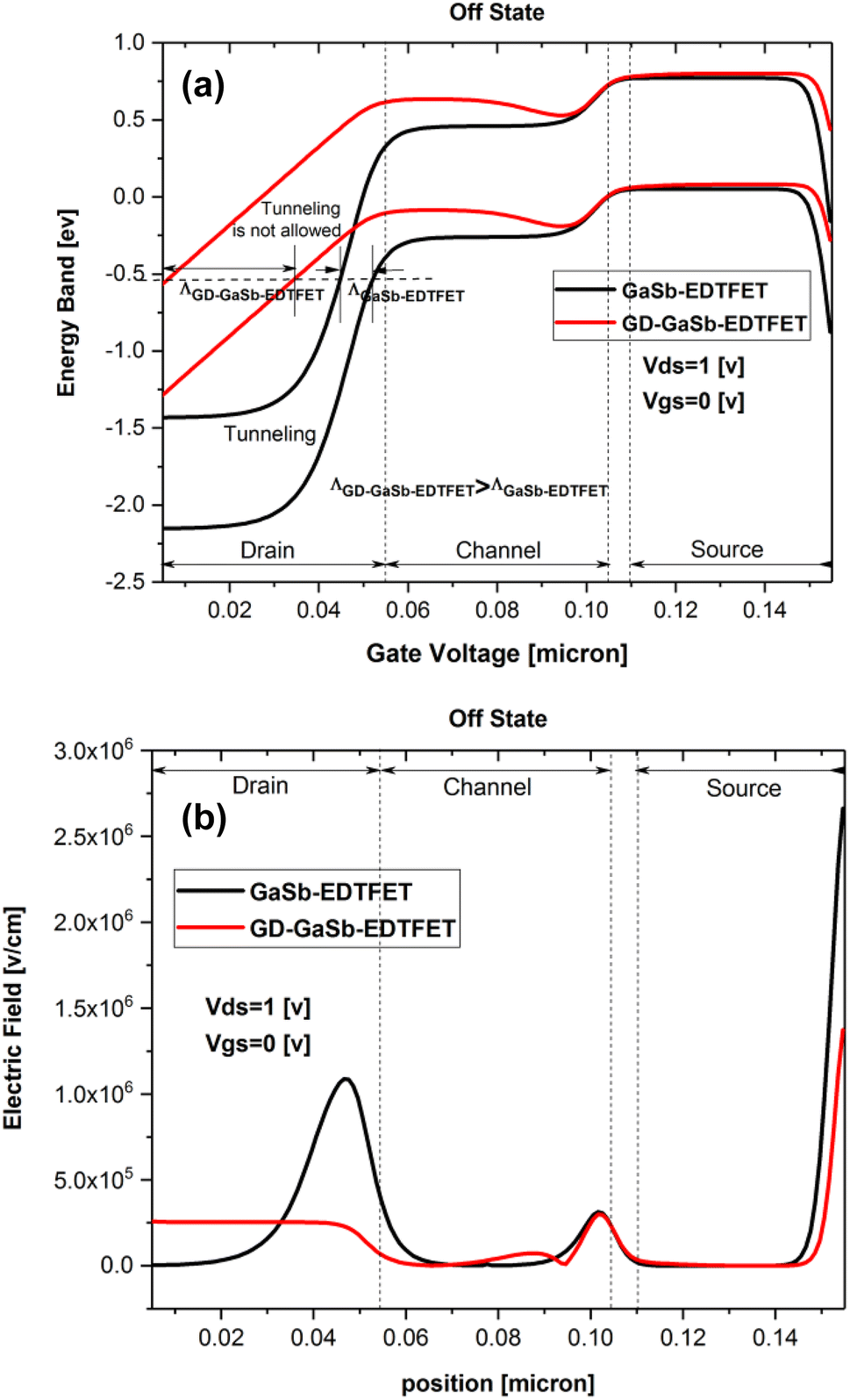
The decrease of the off and ambipolar current by applying Gaussian doping to GaSb–EDTFET device (GD–GaSb–EDTFET) is shown in Fig.
5
. Energy band diagram of the structures at off state, wherein gate voltage is zero, is represented in Fig.
6
a. It illustrates that no overlap happens between the conduction band of the channel and the valence band of the source. It is also observed that the tunneling barrier length is higher by applying Gaussian doping. Therefore, at off state, according to Eq. (
1
), the probability of the tunneling is diminished, and consequently, the current is reduced. Similarly, it accrues at ambipolar state. The electric field is obtained from the gradient of the energy band diagram. As can be seen in Fig.
6
b, there are two peaks at source/channel and drain/channel interfaces in the electric field profile of GaSb–EDTFET, because the doping profile is N
+
–I–P
+
. In the GD–GaSb–EDTFET, the gradient of the energy band diagram at drain/channel interface is neglected due to Gaussian-doping profile; consequently, the electric field profile at this interface is negligible; therefore, the off current is reduced. The ambipolar performance is also similar to off state.
Fig. 5
Comparison of the conventional Si-EDTFET, GaSb–EDTFET and GD–GaSb–EDTFET transfer characteristics at Vds = 1.0 V
Fig. 6
Comparison of GaSb–EDTFET and GD–GaSb–EDTFET at the off state.
a
Energy band diagram.
b
Electric field profile
The performance of the device in the subthreshold region is often based on the subthreshold swing. Point subthreshold swing (SS
p
) represents the reverse of the slope of the transfer characteristic under log scale for Ids. Since the average subthreshold swing (SS
ave
) is independent of the step size of gate voltage, it is more common to use. The entire range of gate voltage up to threshold voltage (
Vth
) is used to calculate SS
ave
, according to Eq. (
4
) [
13
,
19
]:
SSave=Vth-VofflogIDVth-logIoff,
where
Vth
is the threshold voltage obtained at the drain-to-source current which is 10
−7
A/μm [
1
].
Voff
voltage denotes the voltage at Vgs equals to zero. Based on the calculations, in addition to improving the parameters in terms of
Iambipolar
,
Ion
,
Ioff
, and
Ion
/
Ioff
ratios in the GD–GaSb–EDTFET compared to the conventional EDTFET, the threshold voltage and subthreshold swing have also been rectified.
Vth
is 0.6 V and SS
ave
is 56 mV/dec for the GD–GaSb–EDTFET, compared to 0.78 V and 84 mV/dec for the conventional EDTFET.
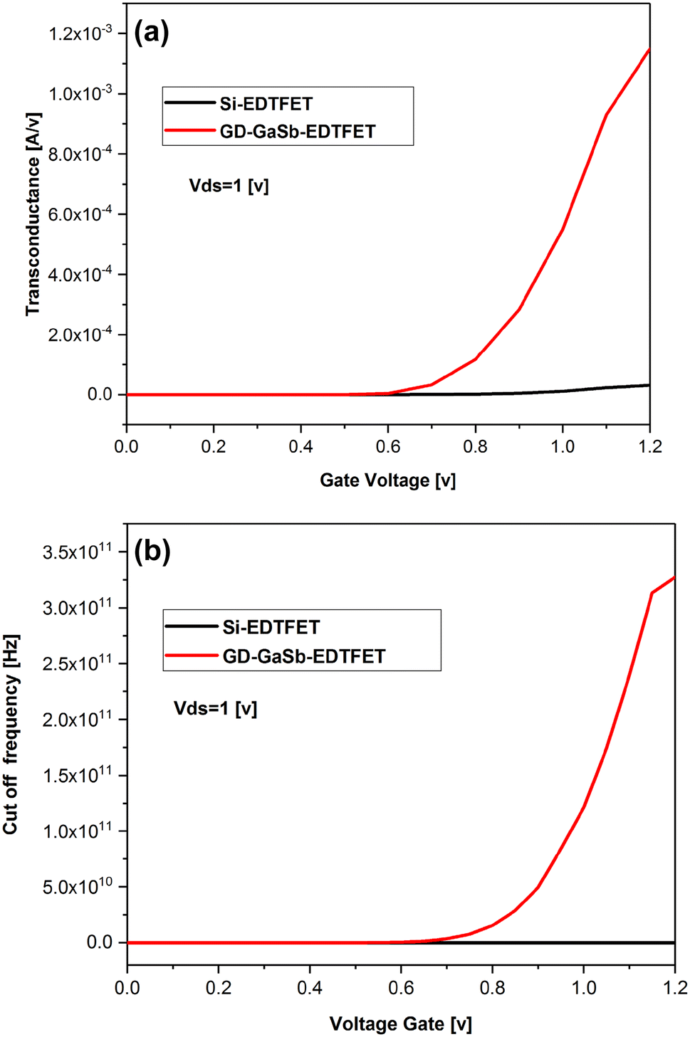
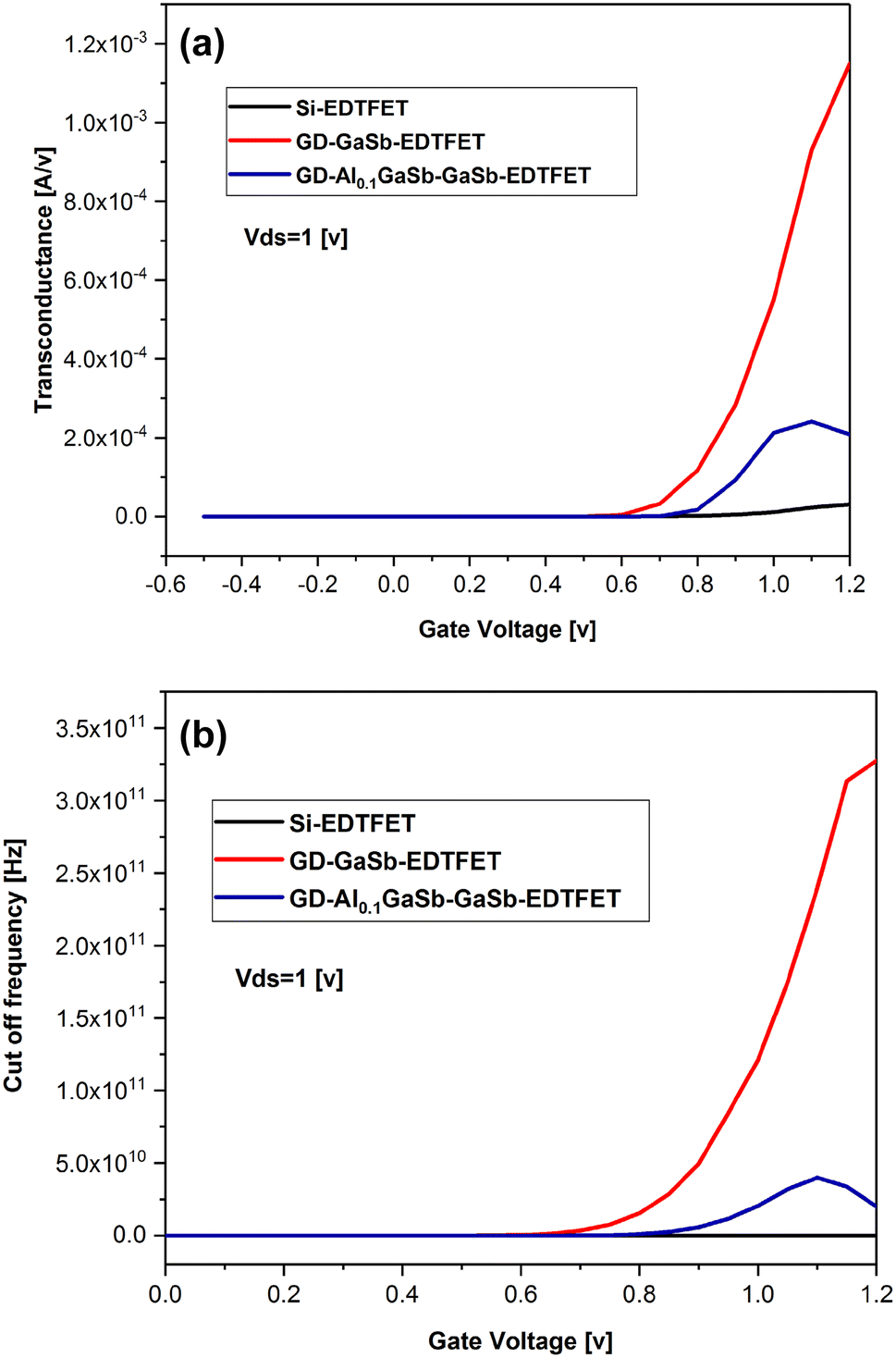
Analog performance
In this section, the analog performance of the GD–GaSb–EDTFET compared to the conventional EDTFET is analyzed. Cut-off frequency (
fT
) and transconductance (gm) of the structures are obtained and compared. The parameter gm is the ratio of the variation in the drain current to the variation in the gate voltage of the device. By increasing the gate–source voltage, the number of electrons injected from the source\channel interface is incremented due to the quantum-tunneling phenomenon; therefore, the gm parameter is increased which has the significant role to determine cut-off frequency.
The parameter
fT
, determined by
fT
= gm/2
π
Cgg, is evoked from a small-signal ac solution at a frequency of 1 MHz, wherein Cgg represents the total gate capacitance and is defined by CG = ∂Qch/∂Vgs. Qch is the total charge in the channel. By assuming a good gate electrostatic control, the parasitic capacitance can be negligible [
61
]. Therefore, it is considered that the charge in the channel and gate is the same. Significantly enhancement analog performance of GD–GaSb–EDTFET is observed in terms of gm and
fT
compared to the conventional EDTFET in Fig.
7
a, b.
Fig. 7
Comparison of the conventional Si-EDTFET and GD–GaSb–EDTFET,
a
transconductance,
b
cut-off frequency
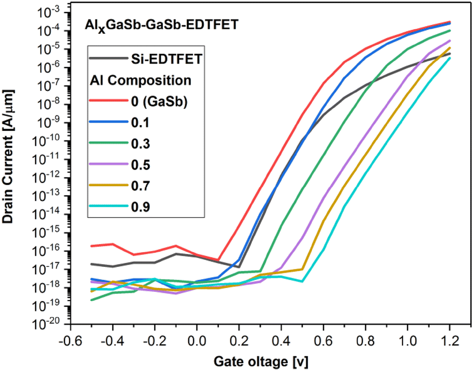
Heterostructure EDTFET
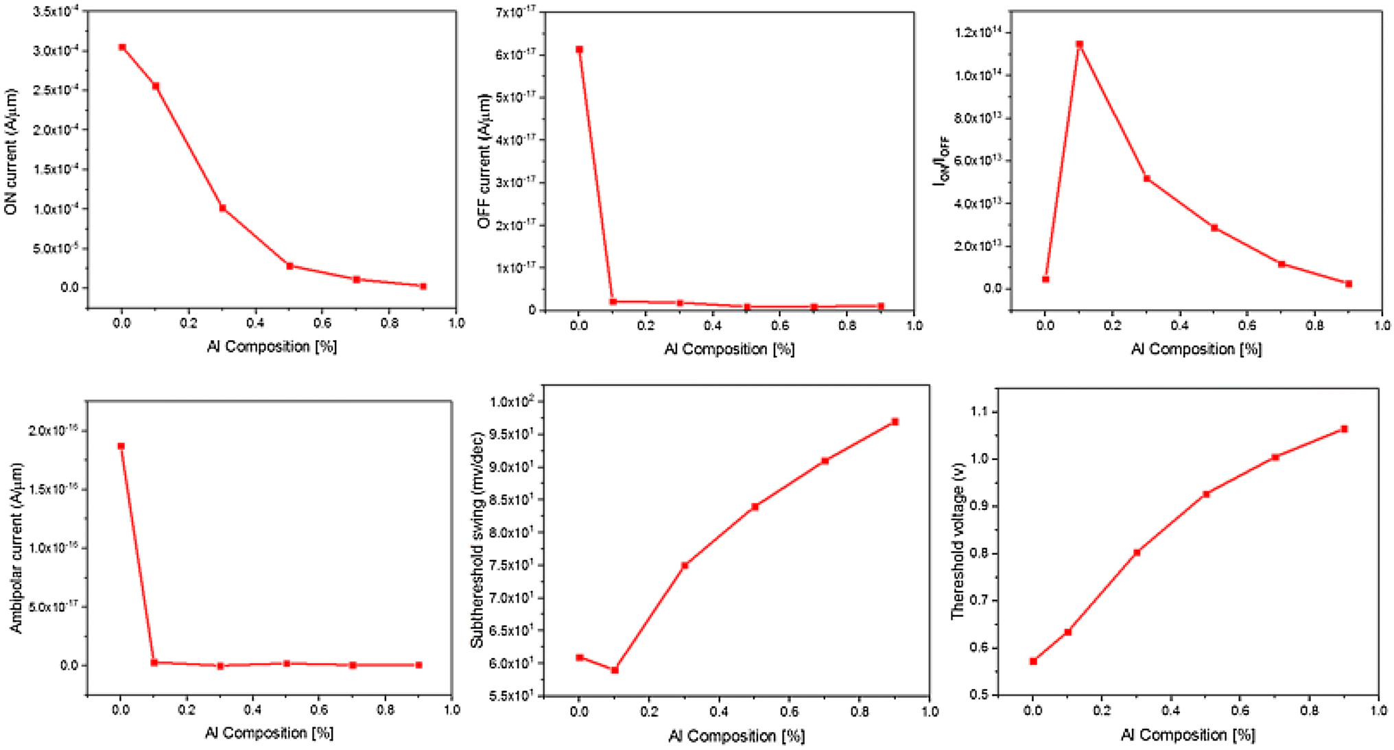
In the previous section, the ambipolar and off current were decreased using the Gaussian-doping profile. In the rest of this research, heterostructure channel/source interface EDTFET is investigated. Heterostructure TFETs employ a low bandgap material at the source region resulting in the improved on-current. However, the ambipolar behavior can be suppressed using a wide bandgap material at the source and drain side. Therefore, the AlGaSb at the channel and drain side and the GaSb at source side are chosen with the uniformly doping profile. To optimize the performance of the heterostructure device, more mole fraction x of aluminum is investigated in the drain and channel side as Al
x
Ga
1-
x
Sb. By increasing the Al fraction, the bandgap energy of Al
x
Ga
1-
x
Sb becomes larger, and as a result, the tunneling probability at the channel/drain interface decreases according to Eq. (
1
). The transfer characteristic of the heterostructure EDTFET with different Al composition (x) values is presented in Fig.
8
. It is observed that, by the increment of the value of
x
, off current is effectively reduced and consequently suppressed the ambipolar behavior because of gate-induced drain leakage (GIDL) at the drain and channel junction. The extracted
Ion
,
Ioff
,
Ion
/
Ioff
ratio,
Iamb
, SS
ave,
and
Vth
as a function of Al composition are illustrated in Fig.
9
. It is explicit that
Ion
,
Ioff,
and I
amb
reduce by increasing of mole fraction
x
. Therefore, higher
Ion
, lower
Iamb,
and
Ioff
cannot occur at the same time. Hence, by trading-off between the above parameters, Al mole fraction is chosen 10% (
x
= 0.1). In spite of reducing on-current by increasing Al mole fraction, as shown in Fig.
8
,
Ion
is still improved compared to the conventional Si-EDTFET, in addition to reduce
Ioff
,
Iamb
by selecting 0.1 for Al mole fraction. By extracting from the transfer characteristic (Id–Vgs) of Al
0.1
GaSb–GaSb–EDTFET device,
Ion
is 0.25 mA/μm,
Ioff
is 2.2 × 10
−18
A/μm,
Iamb
is 3 × 10
−18
A/μm,
Vth
is 0.63 V, and SS
ave
is 59 mV/dec.
Fig. 8
Comparison of the conventional Si-EDTFET and Al
x
Ga
1-
x
Sb–GaSb–EDTFET transfer characteristics with different Al compositions
Fig. 9
Variations of the
Iamb
,
Ioff
,
Ion
,
Ion
/
Ioff
ratio, SS, and
Vth
versus Al composition of Al
x
Ga
1−
x
Sb–GaSb–EDTFET
In the following, the combination of the two above methods, heterostructure and Gaussian-doping profile, on EDTFET (GD–Al
0.1
GaSb–GaSb–EDTFET) is investigated and DC parameters’ device is obtained using the extract of transfer characteristic (Id-Vgs). SS
p
is 37 mV/dec,
Ion
is 6.2 × 10
−5
A/μm,
Ioff
is 1.7 × 10
−19
A/μm,
Ion
/
Ioff
ratio is 3.6 × 10
14
, and
Iamb
is 1.3 × 10
−23
A/μm. Therefore, it is clear that
Iamb
has declined sharply.
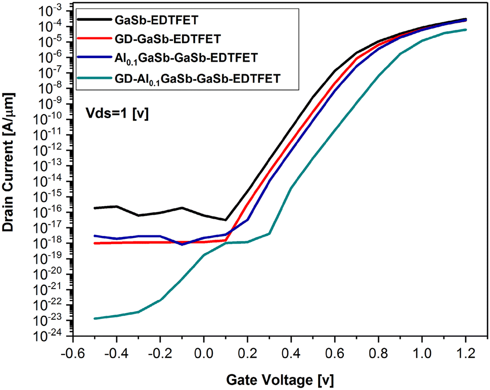
Figure
10
shows a comparison between the two methods and the blend of them based on Id–Vgs curve. As it is explicit from the figure, the method of the applying Gaussian-doping profile, GD–GaSb–EDTFET, and the use of the heterostructure (Al
0.1
GaSb–GaSb–EDTFET) results in almost the same decrease in
Iamb
. However, by combining these two methods, GD–Al
0.1
GaSb–GaSb–EDTFET,
Ioff
is decreased and
Iamb
is sharply reduced. However, from
Ion
and
Vth
point of view, both of them are slightly undermined.
Fig. 10
Comparison of GaSb–EDTFET, GD–GaSb–EDTFET, Al
0.1
GaSb–GaSb–EDTFET, and GD–Al
0.1
GaSb–GaSb–EDTFET transfer characteristics
According to the results obtained in Table
2
,
Ion
,
Ioff
,
Ion
/
Ioff
, Iamb, and
Vth
of both the proposed devices) GD–GaSb–EDTFET and GD–Al
0.1
GaSb–GaSb–EDTFET( have been improved as compared with the conventional Si-EDTFET device; therefore, both the proposed devices are the suitable candidates for analog and digital applications. By the comparison of the two proposed devices with each other and based on the results of Table
2
, transconductance and cut-off frequency curves (Fig.
11
), it can be found that the GD–GaSb–EDTFET is more suitable for analog applications because of higher amounts of
Ion
, gm,
fT,
and
Vth
than those of the GD–Al
0.1
GaSb–GaSb–EDTFET. In addition,
Ioff
,
Iamb
, the
Ion
/
Ioff
ratio, and the SS
P
extracted from the GD–Al
0.1
GaSb–GaSb–EDTFET are better than the GD–GaSb–EDTFET, so the GD–Al
0.1
GaSb–GaSb–EDTFET is the more proper candidate for digital applications.
Table 2
Obtained parameters of the proposed devices and conventional EDTFET
Structures
SS Point (mV/dec)
SS average (mV/dec)
Threshold voltage (V)
Ambipolar current (A/μm)
Off current (A/μm)
On-current (A/μm)
Ion/Ioff
Si-EDTFET
40
84
0.78
3.6 × 10⁻¹⁷
6.7 × 10⁻¹⁷
5.7 × 10⁻⁶
0.8 × 10¹¹
GD–GaSb–EDTFET
40
56
0.6
9.9 × 10⁻¹⁹
1.2 × 10⁻¹⁸
2.5 × 10⁻⁴
2.1 × 10¹⁴
GD–Al0.1GaSb–GaSb–EDTFET`
37
62
0.74
1.3 × 10⁻²³
1.7 × 10⁻¹⁹
6.2 × 10⁻⁵
3.6 × 10¹⁴
Fig. 11
Comparison of conventional Si-EDTFET, GD–GaSb–EDTFET, and GD–Al
0.1
GaSb–GaSb–EDTFET,
a
tranceconductance,
b
cut-off frequency
Conclusion
In this paper, a junctionless tunnel field-effect transistor was simulated based on electrically doped concept using two-dimensional Silvaco TCAD. To increase on-state current, GaSb, a III–V semiconductor, was used which has narrow bandgap and high carrier mobility. On-state current with a value of 0.25 mA/μm at Vds = 1 V and Vgs = 1.2 V in case of GaSb–EDTFET was found to increase significantly compared to the conventional EDTFET. Then, the Gaussian-doping profile was used to reduce
Ioff
and
Iamb
. Wherein
Iamb
is 9.9 × 10
−19
A/μm,
Ioff
is 1.2 × 10
−18
A/μm,
Ion
is 2.5 × 10
−4
A/μm,
Ion
/
Ioff
ratio is 2.1 × 10
14
, and the subthreshold swing (SS) is 56 mV/dec. In the process of improving the performance of the device at both the analog and digital applications, heterostructure source/channel interface was used; therefore, GaSb was allocated to source and AlGaSb to channel and drain regions. Then, the optimal Al composition for AlGaSb was founded to be around 10% (
x
= 0.1) by trading-off DC characteristics. The next Gaussian-doping profile was used in drain and channel. This Gaussian structure called the GD–Al
0.1
GaSb–GaSb–EDTFET has
Iamb
of 1.3 × 10
−23
A/μm,
Ioff
of 1.7 × 10
−19
A/μm,
Ion
of 6.2 × 10
− 5
A/μm, the
Ion
/
Ioff
ratio of 3.6 × 10
14
, and SS of 37 mV/dec, which has a remarkable improvement over the conventional Si-EDTFET.
fT
and gm of devices were also investigated and the results demonstrated that the proposed devices were significantly better as compared with the conventional EDTFET. According to the numerical simulations, these proposed devices can also be the suitable candidates for analog and digital applications.
Publisher's Note
Springer Nature remains neutral with regard to jurisdictional claims in published maps and institutional affiliations.
References
Boucart and Ionescu (2007) Double-gate tunnel FET with high-k gate dielectric 54(7) (pp. 1725-1733) 10.1109/TED.2007.899389
Pal and Dutta (2016) Analytical drain current modeling of double-gate tunnel field-effect transistors 63(8) (pp. 3213-3221) 10.1109/TED.2016.2581842
Ionescu and Riel (2011) Tunnel field-effect transistors as energy-efficient electronic switches 479(7373) (pp. 329-338) 10.1038/nature10679
Kim et al. (2014) High performance tri-gate extremely thin-body InAs-on-insulator MOSFETs with high short channel effect immunity and Vth tunability 61(5) (pp. 1354-1360) 10.1109/TED.2014.2312546
Sharma and Vishvakarma (2013) Precise analytical model for short-channel quadruple-gate gate-all-around MOSFET 12(3) (pp. 378-385) 10.1109/TNANO.2013.2251895
Colinge et al. (2010) Nanowire transistors without junctions 5(3) (pp. 225-229) 10.1038/nnano.2010.15
Bhuwalka et al. (2005) Scaling the vertical tunnel FET with tunnel bandgap modulation and gate workfunction engineering 52(5) (pp. 909-917) 10.1109/TED.2005.846318
Nirschl et al. (2006) Scaling properties of the tunneling field effect transistor (TFET): device and circuit 50(1) (pp. 44-51) 10.1016/j.sse.2005.10.045
Wang et al. (2004) Complementary tunneling transistor for low power application 48(12) (pp. 2281-2286) 10.1016/j.sse.2004.04.006
Choi et al. (2007) Tunneling field-effect transistors (TFETs) with subthreshold swing (SS) less than 60 mV/dec 28(8) (pp. 743-745) 10.1109/LED.2007.901273
Kao et al. (2012) Direct and indirect band-to-band tunneling in germanium-based TFETs 59(2) (pp. 292-301) 10.1109/TED.2011.2175228
Yadav et al. (2016) Impactful study of dual work function, underlap and hetero gate dielectric on TFET with different drain doping profile for high frequency performance estimation and optimization (pp. 36-46) 10.1016/j.spmi.2016.04.027
Rahi et al. (2017) Heterogate junctionless tunnel field-effect transistor: future of low-power devices 16(1) (pp. 30-38) 10.1007/s10825-016-0936-9
Abdi and Kumar (2014) Controlling ambipolar current in tunneling FETs using overlapping gate-on-drain 2(6) (pp. 187-190) 10.1109/JEDS.2014.2327626
Vladimirescu et al. (2012) An analysis on the ambipolar current in Si double-gate tunnel FETs (pp. 67-72) 10.1016/j.sse.2011.11.009
Nigam and Sharma (2016) Approach for ambipolar behaviour suppression in tunnel FET by workfunction engineering 11(8) (pp. 460-464) 10.1049/mnl.2016.0178
Madan and Chaujar (2017) Gate drain underlapped-PNIN-GAA-TFET for comprehensively upgraded analog/RF performance (pp. 17-26) 10.1016/j.spmi.2016.12.034
Vijayvargiya and Vishvakarma (2014) Effect of drain doping profile on double-gate tunnel field-effect transistor and its influence on device RF performance (pp. 974-981) 10.1109/TNANO.2014.2336812
Raad et al. (2016) Dielectric and work function engineered TFET for ambipolar suppression and RF performance enhancement 52(9) (pp. 770-772) 10.1049/el.2015.4348
Ghosh et al. (2013) A junctionless tunnel field effect transistor with low subthreshold slope 12(3) (pp. 428-436) 10.1007/s10825-013-0450-2
Goswami et al. (2014) Analog performance of Si junctionless tunnel field effect transistor and its improvisation using III–V semiconductor 4(21) (pp. 10761-10765) 10.1039/c3ra46535g
Ghosh and Akram (2013) Junctionless tunnel field effect transistor 34(5) (pp. 584-586) 10.1109/LED.2013.2253752
Anand et al. (2016) Performance analysis of charge plasma based dual electrode tunnel FET 37(5) 10.1088/1674-4926/37/5/054003
Rahi and Ghosh (2015) High-k double gate junctionless tunnel FET with a tunable bandgap 5(67) (pp. 54544-54550) 10.1039/C5RA06954H
Nigam et al. (2017) A barrier controlled charge plasma-based TFET with gate engineering for ambipolar suppression and RF/linearity performance improvement 64(6) (pp. 2751-2757) 10.1109/TED.2017.2693679
Akram et al. (2014) P-type double gate junctionless tunnel field effect transistor 35(1) 10.1088/1674-4926/35/1/014002
Nigam et al. (2017) Performance estimation of polarity controlled electrostatically doped tunnel field-effect transistor 12(4) (pp. 239-244) 10.1049/mnl.2016.0729
Nigam et al. (2016) A new approach for design and investigation of junction-less tunnel FET using electrically doped mechanism (pp. 1-7) 10.1016/j.spmi.2016.07.016
Lahgere et al. (2015) Electrically doped dynamically configurable field-effect transistor for low-power and high-performance applications 51(16) (pp. 1284-1286) 10.1049/el.2015.0079
Anand and Sarin (2016) Analog and RF performance of doping-less tunnel FETs with Si0.55Ge0.45 source 15(3) (pp. 850-856) 10.1007/s10825-016-0859-5
Kumar and Janardhanan (2013) Doping-less tunnel field effect transistor: design and investigation 60(10) (pp. 3285-3290) 10.1109/TED.2013.2276888
Cecil and Singh (2017) Influence of Germanium source on dopingless tunnel-FET for improved analog/RF performance (pp. 244-252) 10.1016/j.spmi.2016.11.039
Thathachary et al. (2014) Electron transport in multigate Inx Ga1–xAs nanowire FETs: from diffusive to ballistic regimes at room temperature 14(2) (pp. 626-633) 10.1021/nl4038399
Lahgere et al. (2016) Dopingless ferroelectric tunnel FET architecture for the improvement of performance of dopingless n-channel tunnel FETs (pp. 16-25) 10.1016/j.spmi.2016.05.004
Abadi and Ziabari (2016) Representation of type I heterostructure junctionless tunnel field effect transistor for high-performance logic application 122(6) 10.1007/s00339-016-0151-3
Rahi et al. (2015) Temperature effect on hetero structure junctionless tunnel FET 36(3) 10.1088/1674-4926/36/3/034002
Asthana et al. (2015) Improved performance of a junctionless tunnel field effect transistor with a Si and SiGe heterostructure for ultra low power applications 5(60) (pp. 48779-48785) 10.1039/C5RA03301B
Gundapaneni et al. (2014) Improved Performance of Junctionless Tunnel FETs with Source/Channel Heterostructure (pp. 289-290) Springer International Publishing 10.1007/978-3-319-03002-9_73
Unknown ()
Tirkey et al. (2017) Investigation of gate material engineering in junctionless TFET to overcome the trade-off between ambipolarity and RF/linearity metrics (pp. 307-315) 10.1016/j.spmi.2017.03.059
Abadi and Ziabari (2016) Improved performance of nanoscale junctionless tunnel field-effect transistor based on gate engineering approach 122(11) 10.1007/s00339-016-0530-9
Bal et al. (2014) Dual material gate junctionless tunnel field effect transistor 13(1) (pp. 230-234) 10.1007/s10825-013-0505-4
Bashir et al. (2015) A high performance gate engineered charge plasma based tunnel field effect transistor 14(2) (pp. 477-485) 10.1007/s10825-015-0665-5
Rahimian and Fathipour (2017) Improvement of electrical performance in junctionless nanowire TFET using hetero-gate-dielectric (pp. 142-152) 10.1016/j.mssp.2016.12.011
Anand and Sarin (2017) Dual material gate doping-less tunnel FET with hetero gate dielectric for enhancement of analog/RF performance 38(2) 10.1088/1674-4926/38/2/024001
Raad et al. (2016) Performance investigation of bandgap, gate material work function and gate dielectric engineered TFET with device reliability improvement (pp. 138-146) 10.1016/j.spmi.2016.04.016
Ram and Abdi (2015) Dopingless PNPN tunnel FET with improved performance: design and analysis (pp. 430-437) 10.1016/j.spmi.2015.02.024
Goswami et al. (2015) Junctionless tunnel field effect transistor with nonuniform doping 14(03) 10.1142/S0219581X14500252
Aghandeh and Ziabari (2017) Gate engineered heterostructure junctionless TFET with Gaussian doping profile for ambipolar suppression and electrical performance improvement (pp. 103-114) 10.1016/j.spmi.2017.06.018
Ahish et al. (2016) Device and circuit level performance analysis of novel InAs/Si heterojunction double gate tunnel field effect transistor (pp. 119-130) 10.1016/j.spmi.2016.04.008
Visciarelli et al. (2016) Impact of strain on tunneling current and threshold voltage in III–V nanowire TFETs 37(5) (pp. 560-563) 10.1109/LED.2016.2539389
Abadi and Ziabari (2016) Representation of strained gate-all-around junctionless tunneling nanowire filed effect transistor for analog applications (pp. 12-16) 10.1016/j.mee.2016.04.016
Yadav et al. (2017) Comparative investigation of novel hetero gate dielectric and drain engineered charge plasma TFET for improved DC and RF performance (pp. 123-133) 10.1016/j.spmi.2017.06.016
Yadav et al. (2016) A novel gate and drain engineered charge plasma tunnel field-effect transistor for low sub-threshold swing and ambipolar nature 100(266) (pp. 266-273) 10.1016/j.spmi.2016.09.029
Yogesh et al. (2017) Nanoscale III–V on Si-based junctionless tunnel transistor for EHF band applications 38(5)
Asthana et al. (2014) Optimal design for a high performance H-JLTFET using hfo2 as a gate dielectric for ultra low power applications 4(43) (pp. 22803-22807) 10.1039/C4RA00538D