Department of Mechanical Engineering, Khulna University of Engineering and Technology, Khulna, 9203, BD
Department of Industrial Engineering and Management, Khulna University of Engineering and Technology, Khulna, 9203, BD
Department of Mechanical Engineering, Bangladesh University of Engineering and Technology, Dhaka, 1000, BD
Abstract
Graphene, a two-dimensional material of sp
2
hybridization carbon atoms, has fascinated much attention in recent years owing to its extraordinary electronic, optical, magnetic, thermal, and mechanical properties as well as large specific surface area. For the tremendous application of graphene in nano-electronics, it is essential to fabricate high-quality graphene in large production. There are different methods of generating graphene. This review summarizes the exfoliation of graphene by mechanical, chemical and thermal reduction and chemical vapor deposition and mentions their advantages and disadvantages. This article also indicates recent advances in controllable synthesis of graphene, illuminates the problems, and prospects the future development in this field.
Introduction
Carbon is a ubiquitous material that has been ever found whereas the epoch making material graphene is also an allotropy of carbon. Actually graphene is a two-dimensional, single-layer sheet of sp
2
hybridized carbon atoms and has arrested enormous attention and research motives for its versatile properties. In sp
2
hybridized bond, the in-plane σ
C–C
bond is one of the strongest bonds in materials and the out-of-plane is π bond, which imparts to a delocalized network or array of electrons resulting electron conduction by providing weak interaction among graphene layers or between graphene and substrate. Graphene is a material which has a large theoretical specific surface area (2630 m
2
g
−1
), high intrinsic mobility (200,000 cm
2
v
−1
s
−1
), [
1
,
2
] high Young’s modulus (∼1.0 TPa) [
3
] and thermal conductivity (∼5000 Wm
−1
K
−1
), [
4
] and its optical transmittance (∼97.7 %) and good electrical conductivity merit attention as well as ability to with stand current density of 108 A/cm
2
[
5
], for applications such as for transparent conductive electrodes [
6
,
7
] among many other potential applications. However, its applicability cannot be effectively realized unless superficial techniques to synthesize high-quality, large-area graphene are developed in a cost effective way. Besides, a great deal of effort is required to develop techniques for modifying and opening its band structure so as to make it a potential replacement for silicon in future electronics. Graphene has been experimentally studied for over 40 years [
8
–
14
] and measurements of transport properties in micromechanically exfoliated layers [
15
], of graphene grown on (SiC) [
16
], large-area graphene grown on copper (Cu) substrates [
17
], as well as a variety of studies involving the use of chemically modified graphene (CMG) to make new materials [
12
–
21
].
The basic building blocks of all the carbon nanostructures are a single graphitic layer that is covalently functionalized sp
2
bonded carbon atoms in a hexagonal honeycomb lattice which forms 3D bulk graphite, when the layers of single honeycomb graphitic lattices are stacked and bound by a weak van der Waals force. When the single graphite layer forms a sphere, it is well known as zero-dimensional fullerene; when it is rolled up with respect to its axis, it forms a one-dimensional cylindrical structure called a carbon nanotube; and when it exhibits the planar 2D structure from one to a few layers stacked, it is called graphene. One graphitic layer is well known as monoatomic or single-layer graphene and two and three graphitic layers are known as bilayer and tri-layer graphene, respectively. More than 5 layer up to 10 layer graphene is generally called few layer graphene, and ~20–30 layer graphene is referred to as multilayer graphene, thick graphene, or nanocrystalline thin graphite [
22
].
Synthesis of graphene
Synthesis of graphene refers to any process for fabricating or extracting graphene, depending on the desired size, purity and efflorescence of the specific product. In the earlier stage various techniques had been found for producing thin graphitic films. Late 1970’s carbon precipitated in the form of thin graphitic layers on transition metal surfaces [
24
,
25
]. In 1975, few-layer graphite was synthesized on a single crystal platinum surface via chemical decomposition methods, but was not designated as graphene due to a lack of characterization techniques or perhaps due to its limited possible applications [
26
].
In those periods, their electronic properties never were investigated because of the difficulty in isolating and transferring them onto insulating substrates. But in the late 90’s Ruoff and co-workers tried to isolate thin graphitic flakes on SiO
2
substrates by mechanical rubbing of patterned islands on HOPG (Highly Oriented Pyrolytic Graphite) [
13
]. However there was no report on their electrical property characterization. Using a similar method this was later achieved in 2005 by Kim and co-workers and the electrical properties were reported [
27
]. But the real prompt advancement in graphene research began after Geim and co-workers first published their work of isolating graphene on to SiO
2
substrate and measuring its electrical properties. After discovery of graphene in 2004 various techniques were developed to produce thin graphitic films and few layer graphene. The experimental evidence of 2D crystals came in 2004 [
15
] and 2005 [
28
] when thin flakes of graphene and other materials molybdenum disulphide, niobium diselenide and hexagonal boron nitride were first exfoliated from their bulk counterparts (Fig.
1
). But graphene was first obtained in the form of small flakes of the order of several microns through mechanical exfoliation of graphite using scotch tape [
4
,
9
]. Although this method gives the highest quality graphene but for mass production, fabrication method is needed that can synthesize wafer scale graphene.
Fig. 1
Mother of all graphene forms. Graphene is a 2D building material for carbon material of all other dimensionalities. It can be wrapped up into 0D buckyballs, rolled into 1D nanotubes or stacked into 3D graphite [
23
]
In recent years, various techniques have been established for graphene synthesis. However, mechanical cleaving (exfoliation) [
15
], chemical exfoliation [
29
,
30
], chemical synthesis [
21
], and thermal chemical vapor deposition (CVD) [
31
] synthesis are the most commonly used methods today. Some other techniques are also reported such as unzipping nanotube [
32
–
34
] and microwave synthesis [
35
]. Although mechanical exfoliation using AFM cantilever was found capable of fabricating few-layer graphene, the process limitation was thickness of graphene varies to ~10 nm, which is comparable to 30-layer graphene.
In chemical exfoliation method, solution dispersed graphite is exfoliated by inserting large alkali ions between the graphite layers. Chemical synthesis is the similar process which consists of the synthesis of graphite oxide, dispersion in a solution, followed by reduction with hydrazine. Similarly for carbon nanotube synthesis, catalytic thermal CVD has proved most significant process for large-scale graphene fabrication. When the thermal CVD process is carried out in a resistive heating furnace, it is known as thermal CVD, and when the process consists of plasma-assisted growth, it is called plasma enhanced CVD or PECVD. In this world as nothing is unmixed blessing, all synthesis methods have some drawbacks too depending upon the final application of graphene. For instance, the mechanical exfoliation method is capable of fabricating monolayer to few-layers of graphene, but the reliability of obtaining a similar structure using this technique is quite insignificant. Furthermore, chemical synthesis processes are low temperature processes that make it more comfortable to fabricate graphene on multi-types of substrates at ambient temperature, particularly on polymeric substrate. But, large-area synthesized graphene produced in this process are non-uniform and dispersed. Again, graphene synthesized from reduced graphene oxides (RGOs) usually causes incomplete reduction of graphite oxide that results in the successive debasement of electrical properties depending on its degree of reduction. In contrast, thermal CVD methods are more advantageous for large-area device fabrication and favorable for future complementary metal-oxide semiconductor (CMOS) technology by replacing Si [
36
]. Epitaxial graphene means thermal graphitization of a SiC surface which is another method of graphene synthesis, but the limitation of this method are high process temperature and inability to transfer on any other substrates. So, the thermal CVD method is unique because of producing uniform layer of thermally chemically catalyzed carbon atoms and that can be deposited onto metal surfaces and also can be transferred over a wide range of substrates.
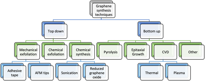
An overview of graphene synthesis techniques is shown in the flow chart in Fig.
2
.
Fig. 2
A process flow chart of Graphene synthesis
Bottom-up graphene
The nature, average size, and thickness of the graphene sheets produced by different bottom-up methods as well as the advantages and disadvantages of each method are summarized in Table
1
.
Table 1
Concise history of Bottom up graphene
Method
Typical dimension
Advantage
Disadvantage
References
Thickness
Lateral
Confined self-assembly
Single layer
100’s nm
Thickness control
Existence of defects
[37]
CVD
Few layer
Very large (cm)
Large size; high quality
Small production scale
[17, 38–42]
Arc discharge
Single, bi and few layers
Few 100 nm to a few μ m
Can produce ~10 g/h of graphene
Low yield of graphene; carbonaceous impurities
[43, 44]
Epitaxial growth on SiC
Few layers
Up to cm size
Very large area of pure graphene
Very small scale
[45–51]
Unzipping of carbon nanotubes
Multiple layers
few μ m long nano ribbons
Size controlled by selection of the starting nanotubes
Expensive starting material; oxidized graphene
[33, 34, 52]
Reduction of CO
Multiple layers
Sub-µm
Un-oxidized sheets
Contamination with α-Al2O3 and α-Al2S
[53]
Top-down graphene
In top-down process, graphene or modified graphene sheets are produced by separation/exfoliation of graphite or graphite derivatives (such as graphite oxide (GO) and graphite fluoride. Table
2
may surmise some researcher’s contribution.
Table 2
Concise history of Top-down graphene
Method
Typical dimension
Advantage
Disadvantage
References
Thickness
Lateral
Directly from graphite
Micromechanical exfoliation
Few layers
µm to cm
Large size and unmodified graphene sheets
Very small scale production
[15]
Direct sonication of graphite
Single and multiple layers
µm or sub-µm
Unmodified graphene, inexpensive
Low yield; separation
[54, 55]
Electrochemical exfoliation/functionalization of graphene
Single and few layers
500–700 nm
Single step functionalization and exfoliation; high electrical conductivity of the functionalized graphene
Cost of ionic liquids
[56]
Super acid dissolution of graphite
Mostly single layer
300–900 nm
Unmodified graphene; scalable
Use of hazardous chlorosulfonic acid; cost of acid removal
[57]
Mechanical exfoliation
Mechanical exfoliation is may be the rarest and eminent process for extracting single layer graphene flakes on preferred substrates. It is the first recognized method of graphene synthesis. This is a top-down technique in nanotechnology, by which a longitudinal or transverse stress is created on the surface of the layered structure materials. Graphite is formed when mono-atomic graphene layers are stacked together by weak van der Waals forces. The interlayer distance and interlayer bond energy is 3.34 Å and 2 eV/nm
2
, respectively. For mechanical cleaving, ~300 nN/μm
2
external force is required to separate one mono-atomic layer from graphite [
27
]. Stacking of sheets in graphite is the result of overlap of partially filled π orbital perpendicular to the plane of the sheet (involving van der Waals forces). Exfoliation is the reverse of stacking; owing to the weak bonding and large lattice spacing in the perpendicular direction compared to the small lattice spacing and stronger bonding in the hexagonal lattice plane [
58
]. Graphene sheets of different thickness can indeed be obtained through mechanical exfoliation or by peeling off layers from graphitic materials such as highly ordered pyrolytic graphite (HOPG), single-crystal graphite, or natural graphite [
59
–
63
]. This peeling/exfoliation can be done using a variety of agents like scotch tape [
15
], ultrasonication, [
64
] electric field [
65
] and even by transfer printing technique [
66
,
67
], etc. In certain studies the HOPG has also been bonded to the substrate either by regular adhesives like epoxy resin [
64
,
68
] or even by SAMs [
69
] to improve the yield of single and few layer graphene flakes. A recent study also demonstrates transfer printing of macroscopic graphene patterns from patterned HOPG using gold films [
70
]. It is by far the cheapest method to produce high-quality graphene. Graphene flakes obtained by mechanical exfoliation methods are usually characterized by optical microscopy, Raman spectroscopy and AFM. AFM analysis is carried out on exfoliated graphene to assess its thickness and number of layers. Finding a single layer flake is a fact of chance plus the yield of single and few layer graphene obtained by this method is more weaker and the flakes are randomly diffused on the substrate. Optical microscopy is another popular method of identifying single layer graphene. Depending on thickness graphene flakes give a characteristic color contrast on a thermally grown SiO
2
layer of 300 nm thickness on top of Si wafers [
71
]. Raman spectroscopy is also carried out on graphene acquiring by mechanical exfoliation. It is the quickest and most precise method of identifying the thickness of graphene flakes and estimating its crystalline quality. This is because graphene exhibits characteristic Raman spectra based on number of layers present [
72
–
74
]. In this micromechanical exfoliation method, graphene is separated from a graphite crystal using adhesive tape. After peeling it off the graphite, multiple-layer graphene remains on the tape. By repeated peeling the multiple-layer graphene is cleaved into several flakes of few-layer graphene. Subsequently the tape is attached to the acetone substrate for detaching the tape. Finally one last peeling with an unused tape is performed. The obtained flakes vary substantially in size and thickness, where the sizes range from nanometers to several tens of micrometers for single-layer graphene, based on wafer. Single-layer graphene has an absorption rate of 2 %, nevertheless it is possible to see it under a light microscope on SiO
2
/Si, due to interference effects [
75
].
Actually it is not easy to obtain larger amounts of graphene by this exfoliation method, not even taking into account the lack of sustainable flakes. The difficulty of this method is really low, nevertheless the graphene flakes require to be found on the substrate surface, which is labor exhaustive. The quality of the prepared graphene is very high with almost no defects. The graphene formed by these mechanical exfoliation methods was used for production of FET devices (Fig.
3
). Still, the mechanical exfoliation method needs to be enhanced further for large-scale, defect-free, high-purity graphene for mass production in the field of nanotechnology.
Fig. 3
Graphene films.
a
Photograph (in normal white light) of a relatively large multilayer graphene flake with thickness ~3 nm on top of an oxidized Si wafer.
b
Atomic force microscope (AFM) image of 2 µm by 2 µm area of this flake near its edge. Colors:
dark brown
, SiO
2
surface;
orange
, 3 nm height above the SiO
2
surface.
c
AFM image of single-layer graphene. Colors:
dark brown
, SiO
2
surface;
brown–red
(
central area
), 0.8 nm height;
yellow–brown
(
bottom left
), 1.2 nm;
orange (top left
), 2.5 nm.
d
Scanning electron microscope image of FLG (Few layer graphene).
e
Schematic view of the device in (
D
) with permission of [
15
]
Chemical exfoliation
Chemical method is one of the best appropriate method for synthesis of graphene. In chemical method producing colloidal suspension which modify graphene from graphite and graphite intercalation compound. Different types of paper like material [
20
], [
76
–
80
] polymer composites [
18
], energy storage materials [
81
] and transparent conductive electrodes [
82
] have already used chemical method for production of graphene. In 1860 graphene oxide was first manufactured Brodie [
83
], Hummers [
84
] and Staudenmaier [
85
] methods. Chemical exfoliation is a two-step process. At first reduces the interlayer van der Waals forces to increase the interlayer spacing. Thus it forms graphene-intercalated compounds (GICs) [
86
]. Then it exfoliates graphene with single to few layers by rapid heating or sonication. For single-layer graphene oxide (SGO) uses ultrasonication [
84
,
87
–
91
] and various layer thickness using Density Gradient Ultracentrifugation [
92
,
93
]. Graphene oxide (GO) is readily prepared by the Hummers method involving the oxidation of graphite with strong oxidizing agents such as KMnO
4
and NaNO
3
inH
2
SO
4
/H
3
PO
4
[
84
,
94
]. Ultrasonication in a DMF/water (9:1) (dimethyl formamide) mixture used and produced single layer graphene. For this reason interlayer spacing increases from 3.7 to 9.5 Å. For oxidization high density of functional groups, and reduction needs to be carried out to obtain graphene-like properties. Single layer graphene sheets are dispersed by chemical reduction with hydrazine monohydrate [
88
,
90
]. Polycyclic aromatic hydrocarbons (PAHs) [
94
–
96
], has used for synthesis of graphene. Using a dendrict precursor transformed by cyclodehydrogenation and planarization [
97
].produce small domains of graphene. Poly-dispersed hyper branched polyphenylene, precursor give larger flakes [
97
]. The first were synthesized through oxidative cyclodehydrogenation with FeCl
3
[
97
]. Variety of solvents are used to disperse graphene in perfluorinated aromatic solvents [
54
], orthodichloro benzene [
98
], and even in low-boiling solvents such as chloroform and isopropanol [
99
,
100
]. Electrostatic force of attraction between HOPG and the Si substrate use in graphene on SiO
2
/Si substrates [
65
]. Laser exfoliation of HOPG has also been used to prepare FG, using a pulsed neodymium-doped yttrium aluminum garnet (Nd:YAG) laser [
42
,
101
]. Thermal exfoliation and reduction of graphite oxide also produce good-quality graphene, generally referred to as reduced graphene oxide (RGO).
Reduction graphene oxide
Chemical reduction of graphite oxide is one of the conventional procedures to prepare graphene in large quantities [
84
]. Graphite oxide (GO) is usually synthesized through the oxidation of graphite using oxidants including concentrated sulfuric acid, nitric acid and potassium permanganate based on Brodie method [
83
], Staudenmaier method [
85
], Hummers method [
84
]. Another approach to the production of graphene is sonication and reduction of graphene oxide (GO). Addition of H
2
occurs across the alkenes, coupled with the extrusion of nitrogen gas, large excess of NaBH
4
have been used as a reducing agent [
102
]. Other reducing agents used include phenyl hydrazine [
103
], hydroxylamine [
104
], glucose, [
105
] ascorbic acid [
106
], hydroquinone [
107
], alkaline solutions [
108
], and pyrrole [
109
]. GO was formed by the chemical reaction between organic isocyanates and the hydroxyl is shown in Fig.
4
also mention the FT-IR spectra of GO.
Fig. 4
a
Proposed reactions during the isocyanate treatment of GO where organic isocyanates react with the hydroxyl (
left oval
) of graphene oxide sheets to form carbamate and amide functionalities, respectively.
b
FT-IR spectra of GO and isocyanate-treated GO. With permission of [
110
]
Electrochemical reduction is another means to synthesize graphene in large scale [
111
–
113
]. In 1962, first established monolayer flakes of reduced graphene oxide. The graphite oxide solution can then be sonicated in order to form GO nanoplatelets. The oxygen groups can then be removed by using a hydrazine reducing agent, but the reduction process was found to be incomplete, leaving some oxygen remaining. GO is useful because its individual layers are hydrophilic, in contrast to graphite. GO is suspended in water by sonication [
114
,
115
] then deposited on to surfaces by spin coating or filtration to make single- or double-layer graphene oxide. Graphene films are then made by reducing the graphene oxide either thermally or chemically [
87
] a simple one-step, solvo thermal reduction method to produce reduced graphene oxide dispersion in organic solvent [
116
]. The colloidal suspensions of chemically modified graphene (CMG) ornamented with small organic molecules [
117
]. Graphene functionalization with poly (
m
-phenylenevinylene-co-2, 5-dioctoxy-
p
-phenylenevinylene) (PmPV) [
118
], 1,2-distearoyl-sn-glycero-3-phosphoethanolamine-
N
[methoxy (polyethyleneglycol)-5000] (DSPE-mPEG) [
119
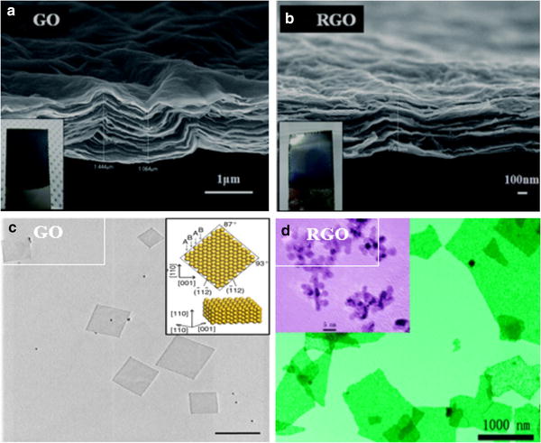
], poly (tert-butyl acrylate). Here two cross-sectional FE-SEM and TEM pictures are shown in Fig.
5
for distinguishing GO and RGO.
Fig. 5
Cross-sectional FE-SEM images of (
a
) graphene oxide (GO) (
b
) Reduced graphene oxide (RGO) with permission of [
120
]. Cross-sectional TEM images of (
c
) graphene oxide (GO) [
121
] (
b
) Reduced graphene oxide (RGO) with permission of [
122
]
Pyrolysis of graphene
Solvo thermal method was used as a chemical synthesis of graphene in bottom up process. In this thermal reaction the molar ratio of sodium and ethanol was 1:1 in closed vessel. Graphene sheets could be smoothly detached by pyrolization of sodium ethoxide using sonication. This produced graphene sheets with dimensions of up to 10 μm. The crystalline structure, different layers, graphitic nature, band structure were inveterate by SAED, TEM and Raman spectroscopy [
123
]. Raman spectroscopy of the resultant sheet showed a broad D-band, G-band, and the intensity ratio of IG/ID ~1.16, representative of defective graphene. The benefits of this process were low-cost and easily fabricated of high-purity, functionalized graphene in low temperature. Yet, the quality of graphene was still not suitable because it comprised a large number of defects.
Chemical vapor deposition (CVD)
Chemical vapor deposition comprises chemical reaction on which process molecules are heated and changed to a gaseous state and that is called precursor. In this CVD process a substrate is diffused on thermally disintegrated precursors in high temperature. It deposits on thin films, crystalline, solid, liquid or gaseous precursors on the surface of the substrate. The deposition of high-quality graphene from CVD process is usually done onto various transition-metal substrates like as Ni [
124
] Pd [
123
], Ru [
49
], Ir [
126
], and Cu [
31
]. CVD growth of graphene has been mainly practiced on copper [
31
,
127
] and nickel [
31
,
124
,
128
] substrates. Nickel was the first substrate on which CVD growth of large area graphene was attempted. These efforts had begun right from 2008. [
129
].In 1966 [
130
] Ni exposed to methane at
T
= 900 °C to form thin graphite, to be used as sample support for electron microscopy. In 1971, they [
131
] observed the formation of FLGs via evaporation of C from a graphite rod [
131
]. Deposition of mono-layer graphitic materials on Pt by thermal CVD was first reported in 1975 [
26
]. Later, Eizenberg and Blakely [
24
] reported graphite layer formation on Ni (111). In 1984 researcher [
132
] performed what may be the first CVD graphene growth on a metal surface, Ir, to study the catalytic and thermionic properties of Ir in the presence of carbon [
133
]. The physical and chemical properties of graphene have been precisely analyzed to open a new area of graphene-based electronics [
15
,
134
–
136
]. In 2006, the first attempt at graphene synthesis on Ni foil using CVD was done using camphor (terpinoid, a white transparent solid of chemical formula C
10
H
16
O) as the precursor material [
137
]. Different hydrocarbons such as methane, ethylene, acetylene, and benzene were decomposed on various transition-metal substrates such as Ni, Cu, Co, Au, and Ru [
31
]. Single crystals using an ethylene precursor was found to yield graphene structurally coherent even over the Ir step edges [
126
]. Using methane as a hydrocarbon Table
3
can emblem a summary of significant researcher’s contribution.
Table 3
Concise illustration of CVD synthesis and characteristics
Cvd synthesis characteristics
Hydrocarbon and other chemical ratio
Temperature
Pressure
Special characteristics
References
Thin layer graphite on Ni
H2: CH4 ≡ 92:8
950 °C
40–80 mT
1–2 nm layer
[129]
DC discharge of the current ~0.5 A/cm2
Graphene formation on polycrystalline Ni
CH4: H2:Ar ≡ 0.15:1:2
1000 °C
1 atm
3–4 layer
[128]
Graphene growth over e-beam evaporated Ni
CH4: H2:Ar ≡550:65:200
1000 °C
_
Large-scale monolayer
[124]
Sheet resistance ~280 ohm/sq
Transmittance 80 %
Graphene formation on polycrystalline Ni by wet-etching
Flow rate Ar and H2 10-20 min
900–1000 °C
_
[31]
Gram-scale graphene using MgO catalyst
CH4:Ar ≡ 1:4 Flow rate 375 l/min
1000 °C
40 m Torr
5-layer graphene sheet
[38]
Substrate free
Catalytic graphene deposition on Cu
2 sccm flow rate
1000 °C
40 m Torr
Single, double and triple layer graphene
[17]
35 sccm flow rate
1000 °C
500 m Torr
Graphene growth using 15 cm × 5 cm
Rectangular Cu foil
H2: CH4 ≡ 1:4
1000 °C
_
_
[138]
Roll-to-roll production of graphene on a flexible polymer
Annealing of Cu in a H2 environment
1000 °C
90 mT
_
[139]
Using precursor CH4 and H2 (3:1)
1000 °C
460 mT
cooling of the furnace
10 °C/min under H2 flow
90 mT
Classification of CVD process
Depending on the material quality, precursors, the width, and the structure required; there are many various types of CVD processes: thermal, plasma enhanced (PECVD), cold wall, hot wall, reactive, and so on.
In CVD process reactors like hot wall reactor, there temperature is relatively constant everywhere and these walls never get heated in cold wall system. Graphene is formed on Cu thin film mostly by cold wall system.
Growth on Cu
Graphene growth on copper shows that it may emerge as alternate route towards scalable growth of graphene with higher monolayer coverage [
17
,
140
]. In 2009, the first CVD growth of uniform as well as large area (~cm
2
) graphene on a metal surface was done on polycrystalline Cu foils by exploiting thermal catalytic decomposition of methane [
17
]. Copper foil was an even superior substrate for growing single layer graphene films [
17
]. Although copper is an inexpensive substitute in contrast to other metals that is also simply extractable by etchants without chemically affecting graphene. For a very small solubility of carbon in copper, the carbon deposition process was found to be largely self-limiting [
17
]. The solubility of carbon in copper is negligible of the perspective of ppm even at 1000 °C [
141
] so the carbon precursor forms graphene directly on copper surface through growth step [
17
]. Cu surface is fully enclosed with graphene, save around 5 % of the comprising of BLG and 3LG [
17
,
142
] area (Fig.
6
). Surface roughness is known to produce graphene thickness variation on copper [
143
,
144
]. Since graphene growth on copper is surface limited, so smoothness of copper surface imparts very significant role in receiving monolayer coverage across the whole surface of the substrate [
145
].
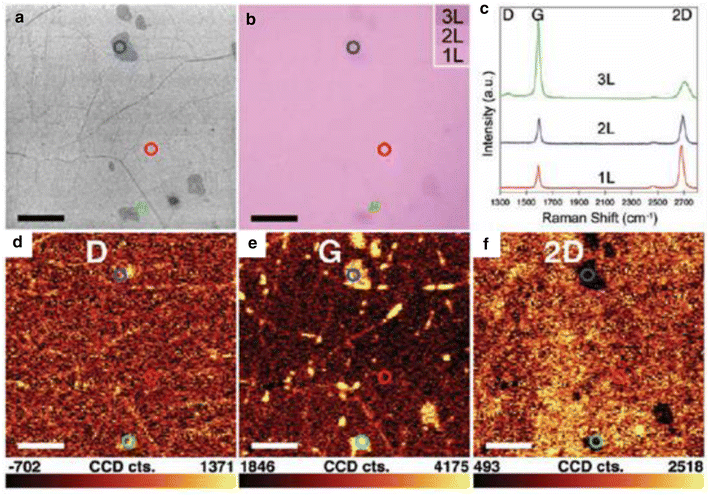
Fig. 6
a
Optical image of as grown graphene on copper, the corrugations on metal foil are indicated by
black arrows
.
b
Same graphene when shifted to 300 nm SiO
2
. Here
dark purple
areas highlighted by
black arrows
displays that even on low carbon solubility metal like copper, corrugations on starting substrate can result in formation of significant multilayer regions along with monolayer graphene [
45
]. Li et al. used CVD process to produce large-scale monolayer graphene on copper foils. 25 μm thick copper foils were first heated to 1000
◦
C in a flow of 2 sccm (standard cubic centimeters per minute) hydrogen at low pressure and then exposed to methane flow of 35 sccm and pressure of 500mTorr and acquired sheet resistances of 125Ω/W for a single layer. Using a repeated transfer method, doped 4-layer graphene sheets were formed with sheet resistances as low as 30Ω/W and optical transmittance greater than 90 %. These 4-layer graphene sheets are better to commercially accessible indium tin oxide (ITO). Permission from [
146
]
Again Li et al. have shown at 1035 °C with methane flow of 7 sccm and pressure 160 m Torr led to the largest graphene domains with average areas of 142 μm
2
. Using this technique, they were able to produce samples with carrier mobility of up to 16,000 cm
2
V
−1
s
−1
[
147
]. Usually, the graphene layer is slightly strained on the copper foil because of the high-temperature growth [
148
] (Fig.
7
). Formation of graphene on Cu by LPCVD was then scaled up in 2010 where, growing the Cu foil size (30 inches), generating films with μ ~ 7350 cm
2
V
−1
s
−1
at 6 K. Large grain, ~20–500 μm, graphene on Cu with μ ranging from ~16,400 to ~25,000 cm
2
V
−1
s
−1
at RT after transfer to SiO
2
was reported in references [
147
,
149
] and from ~27,000 to ~45,000 cm
2
V
−1
s
−1
on h-BN at RT [
149
]. Graphene was also formed on Cu by exposing it to liquids or solid hydrocarbons [
150
,
151
] reported growth using benzene in the T range 300–500 °C. However based on recent studies on CVD growth on copper have demonstrated copper to be a more auspicious substrate [
17
].
Fig. 7
Raman spectroscopy and SEM imaging of single layer graphene grown on copper (With Permission) [
17
]
Growth on Ni
Due to few disturbing properties of Cu like surface roughening and sublimation; the researcher had to search for new substrates that was Ni substituting the Cu. Graphene was synthesized by Ni foil, polycrystalline nickel thin film, patterned Ni thin film [
152
].
The foils were first annealed in hydrogen and then bare to a CH
4
–Ar–H
2
environment at atmospheric pressure for 20 min at a temperature of 1000 °C [
128
].The thickness of the graphene layers was found to be reliant on the cooling rate, with few layer graphene. Faster cooling rates consequence in thicker graphite layers, whereas slower cooling avoids carbon from separating to the surface of the Ni foil [
128
]. Still, the T range within which graphene can be grown on Ni is very thin, 100 °C [
153
], and could end in a Ni 2C phase [
153
], which can give rise to defects within the Ni crystal. In a nutshell any graphene grown on the surface could be non-uniform through the Ni–Ni2C regions (Fig.
8
). The problems of Ni synthesis were time-consuming exposure to the carbon precursor, not self-limiting, catalyzed growth with large number of wrinkles and folds.
Fig. 8
SEM images of sample by CVD growth method on Ni film at 900–1000 °C at various H
2
:CH
4
ratios with permission of [
154
]
Plasma-enhanced chemical vapor deposition
Plasma-enhanced chemical vapor deposition (PECVD) generates plasma in void chamber which deposits thin flim on the substrate surface. It comprises with chemical reaction of the reacting gases.IN PECVD system uses RF (AC frequency), microwave, and inductive coupling (electrical currents produced by electromagnetic induction). It can be done at relatively low temperature, more feasible for large-scale industrial application and also catalyst free graphene fabrication [
155
]. Though it is costly and gas-phase precursor materials are used. The first synthesis of graphene sheets was established [
156
]. The production of mono- and few layer of graphene by PECVD on different substrates like Si, SiO
2
, Al
2
O
3
, Mo, Zr, Ti, Hf, Nb, W, Ta, Cu, and 304 stainless steel. Using 900-watt RF power, 10 sccm total gas flow, and inside chamber pressure of ~12 Pa, gas mixture 5–100 % CH
4
in H
2
and 600–900 substrate temperature [
157
]. The plasma was deposited within 5–40 min. For complementary metal-oxide semiconductor (CMOS) devices it is need to reduce the temperature. PECVD reduces temperature during deposition was widely exploited in the growth of nanotubes and amorphous carbon [
158
–
163
]. When at
T
= 317 °C to make TCs with Rs ~ 2 kΩ/at 78 % transmittance. Inductively coupled plasma (ICP) CVD, was used to grow graphene on 150 mm Si wafers [
164
], reaching uniform films and good transport properties (i.e., μ up to ~9000 cm
2
V
−1
s
−1
).
Epitaxial growth of graphene
Epitaxial thermal growth on a single crystalline silicon carbide (SiC) surface is one of the most praised methods of graphene synthesis. The term “epitaxy” derives from the Greek, the prefix epi means “over” or “upon” and taxis means “order” or “arrangement”. When the deposition of a single crystalline film on a single crystalline substrate produces epitaxial film and the process is known as epitaxial growth. It fabricates high-crystalline graphene onto single-crystalline SiC substrates. There are two general epitaxial growth processes depending on the substrate, homo-epitaxial and hetero-epitaxial growth. When the film deposited on a substrate is of the same material it is known as a homo-epitaxial layer, and if the film and substrate are different materials it is called a hetero-epitaxial layer. Sic first used as on electrical measurements on patterned epitaxial graphene on electrical measurements on patterned epitaxial graphene. In 2004 [
16
] SiC is a wide band gap semiconductor (3 eV) and thus electrical measurements can be carried out using it as the substrate. In 1975, Bommel et al. [
165
] first reported graphite formation on both the 6H–SiC (0001) surfaces. The heat treatment in the range of 1000–1500 °C in an ultrahigh vacuum (~10–10 m bar) manufactured graphite on both of the SiC polar planes (0001). In 2004, de Heer’s [
166
] group reported the fabrication of ultrathin graphite consisting of 1–3 mono-atomic graphene layers on the Si completed (0001) face of single-crystal 6H-SiC and explored its electronic properties [
167
]. The growth rate of graphene on SiC depends on the specific polar SiC crystal face [
166
,
167
]. Graphene forms much faster on the C- than on the Si-face [
166
,
167
]. On the C-face, larger domains (~200 nm) of multilayered, rotationally disordered graphene are produced [
167
,
168
]. On the Si-face, UHV annealing leads to small domains, ~30–100 nm [
168
,
169
]. (Si (0001)- and C (000-1)-terminated) annealed at high
T
(>1000 °C) under ultra-high vacuum (UHV) graphitize due to the evaporation of Si [
170
,
171
]. Graphene films by thermal decomposition of SiC above1000 °C, graphene grows on a C-rich 6√3 × 6√3R30° rebuilding with respect to the SiC surface [
172
,
181
]. Epitaxial graphene growth on SiC has been visualized as a very promising method for large-scale production and commercialization of graphene for applications into electronics. Graphene on SiC produces high-frequency electronics [
173
], light emitting devices [
173
], and radiation hard devices [
173
]. Top gated transistors have been fabricated from graphene on SiC on a wafer scale [
174
]. High-frequency transistors have also been revealed with 100 GHz cut-off frequency208 [
175
], higher than state of the art Si transistors of the same gate length [
176
]. Graphene on SiC has been established as a novel resistance standard based on the quantum Hall effect (QHE) [
177
]. Though this process is very expensive.
Unzipping method
Chemical and plasma-etched method uses in unzipping a carbon nanotube (CNT). Graphene nano ribbon (GNR) defines a thin elongated strip of graphene which demonstrates straight edges. Transformation of electronic state from semimetal to semiconductor depends on the width of nanaotube [
178
]. Multi-layer graphene or single-layer graphene produces if the starting nanotube is multi-walled or single walled. The width of the nanoribbons thus produced depends on the diameter of the precursor nanotubes. Multi-walled carbon nanotubes (MWNTs) established by lithium (Li) and ammonia (NH
3
). Conversion of graphene nanoribbon from (MWNTs) are shown in Fig.
9
.
Fig. 9
The Images of graphene nanoribbons (GNRs) converted from Multi–wall carbon nanaotubes (MWCNTs) with permission of [
34
]
Liquid NH
3
(99.95 %) and dry tetrahydrofuran (THF) used in growth of (MWNTs) retaining the dry ice bath temperature of −77 °C [
179
]. It was found that ~60 % fully exfoliated and (0–5 %) unexfoliated or partially exfoliated nanotubes of (MWNTs). For Oxidation of CNT’s side wall used H
2
SO
4
, KMnO
4
, and H
2
O
2
in step by step process [
32
]. At the beginning they reported that the MWNT diameter was 40–80 nm and increased up to 100 nm. The step-by-step fabrication process from nanotube to nanoribbon is shown in Fig.
10
.
Fig. 10
A process flow chart of graphene nanoribbon fabrication from a carbon nanotube (CNT) by the plasma etching process with permission of [
34
]
In controlled unzipping technique a pristine MWNT (dia. ~4–18 nm) suspension was put on to a Si substrate pretreated with 3-aminopropyltriethoxysilane. A polymethylmethacrylate (PMMA) solution [
34
]. They established high quality of MWNTs which diameter were ~6–12 nm and step height GNRs were 0.8–2.0 nm. Again single- to few-layer GNRs also depends on the plasma etching time.
Another method for unzipping MWCNTs to GNRs used electric field. An electric field was applied to a single MWNT using a tungsten electrode and perceived that the noncontact end of the MWCNT started unwrapping and forming graphene nanoribbon. The fabrication process of GNRs achieve a high-purity, defect-free controlled synthesis process for scalable device in modern electronics.
Others method
There are several other ways to produce graphene such as electron beam irradiation of PMMA nanofibres [
180
], arc discharge of graphite [
181
], thermal fusion of PAHs [
182
], and conversion of nano diamond [
183
]. Graphene can synthesis by arc discharge method in the presence of H
2
atmosphere with two to three layers having flake size of 100–200 nm [
180
,
184
]. By rapid heating process Arc discharge in an air atmosphere resulted in graphene nano sheets that are ~100–200 nm wide predominantly with two layers [
182
]. The conditions that are favorable for obtaining graphene in the inner walls are high current (above 100 A), high voltage (>50 V), and high pressure of hydrogen (above 200 Torr). The vintage of graphene layer depends strongly on the initial air pressure [
185
]. He and NH
3
atmosphere are also used as arc discharge method [
43
]. In He atmosphere has considered gas pressure and currents to obtain different number of graphene sheets. In molecular beam deposition technique used ethylene gas source which deposited on a nickel substrate. Large-area, high-quality graphene layers were produced dependent on cooling rate.
Applications
In the field of application, the novel 2D material graphene plays a vanguard and outstanding role in this twenty-first century. The applications and applied areas of graphene are so vast that it is too many to describe here. The recent advances in the unique electronics, optical, magnetic, surface area, and mechanical properties of functionalized graphene have emerged new approach of green technology and innovative solution of existing problems like as electronic and photonic applications for ultrahigh-frequency graphene-based devices, nanosized graphene in material science, in ceramics, anode for li-ion battery, supercapacitor, lightweight natural gas tanks, sensors to diagnose diseases and solar cell [
186
]. In October 2014, international wheel producer Vittoria released a new range of bicycle race wheels built from graphene-enhanced composite materials. The new wheels (called Quarno) are the best wheels offered by Vittoria, and are said to be the fastest in the world [
187
]. In September 15th, 2015; the first flight of a UAV part-constructed with graphene have brought a new nano-material that the thinnest material on Earth [
188
]. Recently a group of researcher have developed a range of membrane assemblies for advanced water treatment, including crumpled graphene oxide nanocomposites, which are highly water-permeable, photo reactive and antimicrobial. In future there will be myriad scope for disseminating this research concept [
189
].
Conclusion
Recently graphene the noble material has brought a revolutionary change in the field of nanoelectronics. Its outstanding contribution is not only limited in nanoelectronics but also expanding in medical science, nanorobotics, commercial manufacturing of graphene synthesized products and so on.
Acknowledgments
We express deep sense of gratitude and indebtedness to our project supervisor Md. Nizam Uddin, Assistant Professor, Department of Mechanical Engineering for providing precious guidance, inspiring discussions and constant supervision throughout the course of this work. His help, constructive criticism, and conscientious efforts made it possible to present the work contained in this project. It’s our goodness that in spite of having a tight and busy schedule supervisor has found time to help and guided us. For this, we again express our greatness to him. We are also grateful to those staff who help us directly or indirectly which was very essential to accelerate our work.
References
Bolotin et al. (2008) Ultrahigh electron mobility in suspended graphene (pp. 351-355) 10.1016/j.ssc.2008.02.024
Lee et al. (2008) Measurement of the elastic properties and intrinsic strength of monolayer graphene (pp. 385-388) 10.1126/science.1157996
Balandin et al. (2008) Superior thermal conductivity of single-layer graphene 8(3) (pp. 902-907) 10.1021/nl0731872
Moser et al. (2007) Current-induced cleaning of graphene10.1063/1.2789673
Cai et al. (2009) Large area few-layer graphene/graphite films as transparent thin conducting electrodes10.1063/1.3220807
Li et al. (2009) Transfer of large-area graphene films for high-performance transparent conductive electrodes10.1021/nl902623y
Boehm et al. (1962) The adsorption behavior of very thin carbon films 316(3–4) (pp. 119-127) 10.1002/zaac.19623160303
Boehm et al. (1994) Nomenclature and terminology of graphite intercalation compounds (IUPAC Recommendations 1994) 66(9) (pp. 1893-1901) 10.1351/pac199466091893
Boehm et al. (1986) Nomenclature and terminology of graphite intercalation compounds 24(2) (pp. 241-245) 10.1016/0008-6223(86)90126-0
Wintterlin and Bocquet (2009) Graphene on metal surfaces 603(10–12) (pp. 1841-1852) 10.1016/j.susc.2008.08.037
Vanbommel et al. (1975) LEED and Auger electron observations of the SiC(0001) surface 48(2) (pp. 463-472) 10.1016/0039-6028(75)90419-7
Lu et al. (1999) Tailoring graphite with the goal of achieving single sheets 10(3) (pp. 269-272) 10.1088/0957-4484/10/3/308
Lu et al. (1999) Patterning of highly oriented pyrolytic graphite by oxygen plasma etching10.1063/1.124316
Novoselov et al. (2004) Electric field effect in atomically thin carbon films 306(5696) (pp. 666-669) 10.1126/science.1102896
Berger et al. (2004) Ultrathin epitaxial graphite: 2D electron gas properties and a route toward graphene-based nanoelectronics 108(52) (pp. 19912-19916) 10.1021/jp040650f
Li et al. (2009) Large-area synthesis of high-quality and uniform graphene films on copper foils 324(5932) (pp. 1312-1314) 10.1126/science.1171245
Stankovich et al. (2006) Graphene-based composite materials (pp. 282-286) 10.1038/nature04969
Watcharotone et al. (2007) Graphene–silica composite thin films as transparent conductors (pp. 1888-1892) 10.1021/nl070477+
Dikin et al. (2007) Preparation and characterization of graphene oxide paper (pp. 457-460) 10.1038/nature06016
Park and Ruoff (2009) Chemical methods for the production of graphenes (pp. 217-224) 10.1038/nnano.2009.58
Unknown ()
sA. Geim and Novoselov (2007) The rise of graphene 6(3) (pp. 183-191) 10.1038/nmat1849
Eizenberg and Blakely (1979) Carbon monolayer phase condensation on Ni(111) 82(1–2) (pp. 228-236) 10.1016/0039-6028(79)90330-3
Eizenberg and Blakely (1979) Carbon interaction with nickel surfaces: monolayer formation and structural stability 71(8) 10.1063/1.438736
Lang (1975) A LEED study of the deposition of carbon on platinum crystal surfaces 53(1) (pp. 317-329) 10.1016/0039-6028(75)90132-6
Zhang et al. (2005) Fabrication and electric-field dependent transport measurements of mesoscopic graphite devices10.1063/1.1862334
Allen et al. (2010) Honeycomb carbon: a review of graphene 110(1) (pp. 132-145) 10.1021/cr900070d
Viculis et al. (2003) A chemical route to carbon nanoscrolls 299(5611) 10.1126/science.1078842
Reina et al. (2009) Large area, few-layer graphene films on arbitrary substrates by chemical vapor deposition 9(1) (pp. 30-35) 10.1021/nl801827v
Jiao et al. (2010) Facile synthesis of high-quality graphene nanoribbons 5(5) (pp. 321-325) 10.1038/nnano.2010.54
Kosynkin et al. (2009) Longitudinal unzipping of carbon nanotubes to form graphene nanoribbons 458(7240) (pp. 872-876) 10.1038/nature07872
Jiao et al. (2009) Narrow graphene nanoribbons from carbon nanotubes 458(7240) (pp. 877-880) 10.1038/nature07919
Unknown ()
Sutter (2009) Epitaxial graphene: how silicon leaves the scene 8(3) (pp. 171-172) 10.1038/nmat2392
Zhang et al. (2009) A Strategy for producing pure single-layer graphene sheets based on a confined self-assembly approach 48(32) (pp. 5864-5868) 10.1002/anie.200902365
Wang et al. (2009) Large-scale synthesis of few-layered graphene using CVD 15(1–3) (pp. 53-56) 10.1002/cvde.200806737
Wang et al. (2009) Large area, continuous, few-layered graphene as anodes in organic photovoltaic devices10.1063/1.3204698
Dervishi et al. (2009) Large-scale graphene production by RF-cCVD method (pp. 4061-4063) 10.1039/b906323d
Chong-an et al. (2008) Patterned graphene as source/drain electrodes for bottom-contact organic field-effect transistors 20(17) (pp. 3289-3293) 10.1002/adma.200800150
Chae et al. (2009) Synthesis of large-area graphene layers on poly-nickel substrate by chemical vapor deposition: wrinkle formation 21(22) (pp. 2328-2333) 10.1002/adma.200803016
Li et al. (2009) Large scale synthesis of N-doped multi-layered graphene sheets by simple arc-discharge method 48(1) (pp. 255-259) 10.1016/j.carbon.2009.09.013
Karmakar et al. (2009) A novel approach towards selective bulk synthesis of few-layer graphenes in an electric arc 42(11) 10.1088/0022-3727/42/11/115201
Rollings et al. (2006) Synthesis and characterization of atomically thin graphite films on a silicon carbide substrate 67(9-10) (pp. 2172-2177) 10.1016/j.jpcs.2006.05.010
Sutter et al. (2008) Epitaxial graphene on ruthenium (pp. 406-411) 10.1038/nmat2166
Seyller et al. (2008) Epitaxial graphene: a new material 245(7) (pp. 1436-1446) 10.1002/pssb.200844143
Sprinkle et al. (2009) Epitaxial graphene: the material for graphene electronics 3(6) (pp. A91-A94) 10.1002/pssr.200903180
Hirsch (2009) Unzipping carbon nanotubes: a peeling method for the formation of graphene nanoribbons 48(36) (pp. 6594-6596) 10.1002/anie.200902534
Kim et al. (2009) Preparation of graphene sheets by the reduction of carbon monoxide 47(6) (pp. 1610-1612) 10.1016/j.carbon.2009.02.025
Bourlinos et al. (2009) Liquid-phase exfoliation of graphite towards solubilized graphenes 5(16) (pp. 1841-1845) 10.1002/smll.200900242
Hernandez et al. (2008) High-yield production of graphene by liquid-phase exfoliation of graphite (pp. 563-568) 10.1038/nnano.2008.215
Liu et al. (2008) one-step ionic-liquid-assisted electrochemical synthesis of ionic-liquid-functionalized graphene sheets directly from graphite 18(10) (pp. 1518-1525) 10.1002/adfm.200700797
Behabtu et al. (2010) Spontaneous high-concentration dispersions and liquid crystals of grapheme (pp. 406-411) 10.1038/nnano.2010.86
Unknown ()
Hiura et al. (1994) Role of sp3 defect structures in graphite and carbon nanotubes (pp. 148-151) 10.1038/367148a0
Ebbesen and Hiura (1995) Graphene in 3-dimensions: towards graphite origami 7(6) (pp. 582-586) 10.1002/adma.19950070618
Bernhardt et al. (1998) Formation of superperiodic patterns on highly oriented pyrolytic graphite by manipulation of nanosized graphite sheets with the STM tip 408(1–3) (pp. 86-94) 10.1016/S0039-6028(98)00152-6
Lu et al. (1999) Tailoring graphite with the goal of achieving single sheets 10(3) 10.1088/0957-4484/10/3/308
Roy et al. (1998) Manipulation of graphitic sheets using a tunneling microscope10.1063/1.367257
Ci et al. (2009) Graphene shape control by multistage cutting and transfer 21(44) (pp. 4487-4491) 10.1002/adma.200900942
Liang et al. (2008) Electrostatic force assisted exfoliation of prepatterned few-layer graphenes into device sites 9(1) (pp. 467-472) 10.1021/nl803512z
Liang et al. (2007) Graphene transistors fabricated via transfer-printing in device active-areas on large wafer 7(12) (pp. 3840-3844) 10.1021/nl072566s
Vincent et al. (2008) Large and flat graphene flakes produced by epoxy bonding and reverse exfoliation of highly oriented pyrolytic graphite 19(45) 10.1088/0957-4484/19/45/455601
Liu and Yan (2009) Simple method for the covalent immobilization of graphene 9(9) (pp. 3375-3378) 10.1021/nl901669h
Song et al. (2009) Transfer printing of graphene using gold film 3(6) (pp. 1353-1356) 10.1021/nn9003082
Ni et al. (2007) Graphene thickness determination using reflection and contrast spectroscopy 7(9) (pp. 2758-2763) 10.1021/nl071254m
Ferrari (2007) Raman spectroscopy of graphene and graphite: disorder, electron–phonon coupling, doping and nonadiabatic effects 143(1–2) (pp. 47-57) 10.1016/j.ssc.2007.03.052
Ni et al. (2008) Raman spectroscopy and imaging of graphene 1(4) (pp. 273-291) 10.1007/s12274-008-8036-1
Casiraghi et al. (2007) Rayleigh imaging of graphene and graphene layers 7(9) (pp. 2711-2717) 10.1021/nl071168m
Park et al. (2008) Graphene oxide papers modified by divalent ions—enhancing mechanical properties via chemical cross-linking 2(3) (pp. 572-578) 10.1021/nn700349a
Li et al. (2008) Processable aqueous dispersions of graphene nanosheets (pp. 101-105) 10.1038/nnano.2007.451
Xu et al. (2008) Flexible graphene films via the filtration of water-soluble noncovalent functionalized graphene sheets 130(18) (pp. 5856-5857) 10.1021/ja800745y
Park et al. (2008) Aqueous suspension and characterization of chemically modified graphene sheets 20(21) (pp. 6592-6594) 10.1021/cm801932u
Chen et al. (2008) Mechanically strong, electrically conductive, and biocompatible graphene paper 20(18) (pp. 3557-3561) 10.1002/adma.200800757
Stoller et al. (2008) Graphene-based ultracapacitors 8(10) (pp. 3498-3502) 10.1021/nl802558y
Wang et al. (2008) Transparent, conductive graphene electrodes for dye-sensitized solar cells 8(1) (pp. 323-327) 10.1021/nl072838r
Brodie (1860) Sur le poids atomique du graphite (pp. 466-472)
Hummers and Offeman (1958) Preparation of graphitic oxide 80(6) 10.1021/ja01539a017
Staudenmaier (1898) Verfahren zur Darstellung der Graphitsäure 31(2) (pp. 1481-1487) 10.1002/cber.18980310237
Wu et al. (2010) Two-dimensional carbon nanostructures: fundamental properties, synthesis, characterization, and potential applications10.1063/1.3460809
Marcano et al. (2010) Improved synthesis of graphene oxide 4(8) (pp. 4806-4814) 10.1021/nn1006368
Park et al. (2009) Colloidal suspensions of highly reduced graphene oxide in a wide variety of organic solvents 9(4) (pp. 1593-1597) 10.1021/nl803798y
Allen et al. (2009) Honeycomb carbon: a review of graphene 110(1) (pp. 132-145) 10.1021/cr900070d
Tung et al. (2009) High-throughput solution processing of large-scale graphene (pp. 25-29) 10.1038/nnano.2008.329
Paredes et al. (2008) “Graphene oxide dispersions in organic solvents” 24(19) (pp. 10560-10564) 10.1021/la801744a
Green and Hersam (2009) Emerging methods for producing monodisperse graphene dispersions 1(2) (pp. 544-549) 10.1021/jz900235f
Green and Hersam (2009) Solution phase production of graphene with controlled thickness via density differentiation 9(12) (pp. 4031-4036) 10.1021/nl902200b
Wu et al. (2007) Graphenes as potential material for electronics 107(3) (pp. 718-747) 10.1021/cr068010r
Cai et al. (2010) Atomically precise bottom-up fabrication of graphene nanoribbons (pp. 470-473) 10.1038/nature09211
Yan et al. (2010) Large, solution-processable graphene quantum dots as light absorbers for photovoltaics 10(5) (pp. 1869-1873) 10.1021/nl101060h
Zhi and Mullen (2008) A bottom-up approach from molecular nanographenes to unconventional carbon materials (pp. 1472-1484) 10.1039/b717585j
Hamilton et al. (2009) High-yield organic dispersions of unfunctionalized graphene 9(10) (pp. 3460-3462) 10.1021/nl9016623
ONeill et al. (2011) Graphene dispersion and exfoliation in low boiling point solvents 115(13) (pp. 5422-5428) 10.1021/jp110942e
Hernandez et al. (2009) Measurement of multicomponent solubility parameters for graphene facilitates solvent discovery 26(5) (pp. 3208-3213) 10.1021/la903188a
Qian et al. (2011) Formation of graphene sheets through laser exfoliation of highly ordered pyrolytic graphite10.1063/1.3584021
Shin et al. (2009) Efficient reduction of graphite oxide by sodium borohydride and its effect on electrical conductance 19(12) (pp. 1987-1992) 10.1002/adfm.200900167
Pham et al. (2010) One-step synthesis of superior dispersion of chemically converted graphene in organic solvents (pp. 4375-4377) 10.1039/c0cc00363h
Zhou et al. (2011) Reducing graphene oxide via hydroxylamine: a simple and efficient route to graphene 115(24) (pp. 11957-11961) 10.1021/jp202575j
Zhu et al. (2010) Reducing sugar: new functional molecules for the green synthesis of graphene nanosheets 4(4) (pp. 2429-2437) 10.1021/nn1002387
Zhang et al. (2010) Reduction of graphene oxide viaL-ascorbic acid (pp. 1112-1114) 10.1039/B917705A
Wang et al. (2008) Facile synthesis and characterization of graphene nanosheets 112(22) (pp. 8192-8195) 10.1021/jp710931h
Fan et al. (2008) Deoxygenation of exfoliated graphite oxide under alkaline conditions: a green route to graphene preparation 20(23) (pp. 4490-4493) 10.1002/adma.200801306
Amarnath et al. (2011) Efficient synthesis of graphene sheets using pyrrole as a reducing agent 49(11) (pp. 3497-3502) 10.1016/j.carbon.2011.04.048
Stankovich et al. (2006) Synthesis and exfoliation of isocyanate-treated graphene oxide nanoplatelets 44(15) (pp. 3342-3347) 10.1016/j.carbon.2006.06.004
Guo et al. (2009) A green approach to the synthesis of graphene nanosheets 3(9) (pp. 2653-2659) 10.1021/nn900227d
Sundaram et al. (2008) Electrochemical modification of graphene 20(16) (pp. 3050-3053) 10.1002/adma.200800198
Compton et al. (2011) Chemically active reduced graphene oxide with tunable C/O ratios 5(6) (pp. 4380-4391) 10.1021/nn1030725
McAllister et al. (2007) Single sheet functionalized graphene by oxidation and thermal expansion of graphite 19(18) (pp. 4396-4404) 10.1021/cm0630800
Parades et al. (2008) Graphene oxide dispersions in organic solvents 24(19) (pp. 10560-10564) 10.1021/la801744a
Dubin et al. (2010) A one-step, solvothermal reduction method for producing reduced graphene 4(7) (pp. 3845-3852) 10.1021/nn100511a
Xu et al. (2008) Flexible graphene films via the filtration of water-soluble noncovalent functionalized graphene sheets 130(18) (pp. 5856-5857) 10.1021/ja800745y
Li et al. (2008) Chemically derived, ultrasmooth graphene nanoribbon semiconductors 319(5867) (pp. 1229-1232) 10.1126/science.1150878
Li et al. (2008) Highly conducting graphene sheets and Langmuir-Blodgett films 3(9) (pp. 538-542) 10.1038/nnano.2008.210
W et al. (2014) An interleaved porous laminate composed of reduced graphene oxide sheets and carbon black spacers by in situ electrophoretic deposition 4(1) (pp. 3284-3292) 10.1039/C3RA45979A
Unknown ()
Guo et al. (2010) Three-dimensional Pt-on-Pd bimetallic nanodendrites supported on graphene nanosheet: facile synthesis and used as an advanced nanoelectrocatalyst for methanol oxidation 4(1) (pp. 547-555) 10.1021/nn9014483
Choucair et al. (2009) Gram-scaleproduction of graphene based on solvothermal synthesis andsonication 4(1) (pp. 30-33) 10.1038/nnano.2008.365
Kim et al. (2009) Large-scale pattern growth of graphene films for stretchable transparent electrodes (pp. 706-710) 10.1038/nature07719
Kwon et al. (2009) Growth of semiconducting graphene on palladium 9(12) (pp. 3985-3990) 10.1021/nl902140j
Coraux et al. (2008) Structural coherency of graphene on Ir(111)” 8(2) (pp. 565-570) 10.1021/nl0728874
Wei et al. (2009) Synthesis of N-doped graphene by chemical vapor deposition and its electrical properties 9(5) (pp. 1752-1758) 10.1021/nl803279t
Yu et al. (2008) Graphene segregated on Ni surfaces and transferred to insulators 93(11) 10.1063/1.2982585
Obraztsov et al. (2007) Chemical vapor deposition of thin graphite films of nanometer thickness 45(10) (pp. 2017-2021) 10.1016/j.carbon.2007.05.028
Karu and Beer (1966) Pyrolytic formation of highly crystalline graphite films10.1063/1.1708759
Perdereau and Rhead (1971) LEED studies of adsorption on vicinal copper surfaces 24(2) (pp. 555-571) 10.1016/0039-6028(71)90281-0
Kholin et al. (1984) The nature of the adsorption bond between graphite islands and iridium surface 139(1) (pp. 155-172) 10.1016/0039-6028(84)90014-1
Gall et al. (2000) Intercalation of nickel atoms under two-dimensional graphene film on (111)Ir 38(5) (pp. 663-667) 10.1016/S0008-6223(99)00135-9
Li et al. (2009) Evolution of graphene growth on Ni and Cu by carbon isotope labeling (pp. 4268-4272) 10.1021/nl902515k
Luo et al. (2011) Effect of substrate roughness and feedstock concentration on growth of wafer-scale graphene at atmospheric pressure (pp. 1441-1447) 10.1021/cm1028854
Liu et al. (2011) Synthesis of high-quality monolayer and bilayer graphene on copper using chemical vapor deposition (pp. 4122-4130) 10.1016/j.carbon.2011.05.047
Kim et al. (2012) Activation energy paths for graphene nucleation and growth on Cu (pp. 3614-3623) 10.1021/nn3008965
Congqin et al. (2011) Chemical vapor deposition of graphene (pp. 37-54) Rijeka
Li et al. (2010) Graphene films with large domain size by a two-step chemical vapor deposition process 10(11) (pp. 4328-4334) 10.1021/nl101629g
Unknown ()
Unknown ()
Unknown ()
Li et al. (2011) Low-Temperature growth of graphene by chemical vapor deposition using solid and liquid carbon sources10.1021/nn200854p
Reina et al. (2009) Growth of large-area single- and bi-layer graphene by controlled carbon precipitation on polycrystalline Ni surfaces 2(6) (pp. 509-516) 10.1007/s12274-009-9059-y
Addou et al. (2012) Monolayer graphene growth on Ni(111) by low temperature chemical vapor deposition10.1063/1.3675481
Unknown ()
Shang et al. (2008) Catalyst-free efficient growth, orientation and biosensing properties of multilayer graphene nanoflake films with sharp edge planes 18(21) (pp. 3506-3514) 10.1002/adfm.200800951
Obraztsov et al. (2003) DC discharge plasma studies for nanostructured carbon CVD 12(3–7) (pp. 917-920) 10.1016/S0925-9635(02)00338-2
Wang et al. (2004) Synthesis of carbon nanosheets by inductively coupled radio-frequency plasma enhanced chemical vapor deposition 42(14) (pp. 2867-2872) 10.1016/j.carbon.2004.06.035
Chhowalla et al. (2001) Growth process conditions of vertically aligned carbon nanotubes using plasma enhanced chemical vapor deposition10.1063/1.1410322
Teo et al. (2001) Plasma enhanced chemical vapour deposition carbon nanotubes/nanofibres—how uniform do they grow?10.1088/0957-4484/14/2/321
Hofmann et al. (2005) Surface diffusion: the low activation energy path for nanotube growth10.1103/PhysRevLett.95.036101
Boskovic et al. (2002) Large-area synthesis of carbon nanofibres at room temperature10.1038/nmat755
Moseler et al. (2005) The ultrasmoothness of diamond-like carbon surfaces 309(5740) (pp. 1545-1548) 10.1126/science.1114577
Unknown ()
Van Bommel et al. (1975) LEED and Auger electron observations of the SiC(0001) surface 48(2) (pp. 463-472) 10.1016/0039-6028(75)90419-7
Unknown ()
Heera et al. (2011) Large area and structured epitaxial graphene produced by confinement controlled sublimation of silicon carbide10.1073/pnas.1105113108
Hass et al. (2006) Highly ordered graphene for two dimensional electronics10.1063/1.2358299
Hass et al. (2008) Interface structure of epitaxial graphene grown on 4H-SiC(0001)10.1103/PhysRevB.78.205424
Forbeaux et al. (2000) Solid-state graphitization mechanisms of silicon carbide 6H–SiC polar faces10.1016/S0169-4332(00)00224-5
Hass et al. (2002) Highly-ordered graphene for two dimensional electronics10.1063/1.1498962
Emtsev et al. (2008) Interaction, growth, and ordering of epitaxial graphene on SiC{0001} surfaces: a comparative photoelectron spectroscopy study10.1103/PhysRevB.77.155303
Davis (1991) Thin film deposition and microelectronic and optoelectronic10.1109/5.90132
Kedzierski et al. (2008) Epitaxial graphene transistors on SiC substrates10.1109/TED.2008.926593
Cano-Marquez et al. (2009) Ex-MWNTs:Graphene sheets and ribbons produced by lithium intercalation and exfoliation of carbon nanotubes 9(4) (pp. 1527-1533) 10.1021/nl803585s
Subrahmanyam et al. (2009) Simple method of preparing graphene flakes by an arc-discharge method10.1021/jp900791y
Panchakarla et al. (2009) Boron- and nitrogen-doped carbon nanotubes and graphene10.1016/j.ica.2010.07.057
Wu et al. (2009) Synthesis of graphene sheets with high electrical conductivity and good thermal stability by hydrogen arc discharge exfoliation10.1021/nn900020u