224, Department of Electrical Engineering, NIT Rourkela, Rourkela, Odisha, 769 008, IN
Department of Energy Science and Engineering, Indian Institute of Technology Bombay, Mumbai, 400076, IN
Abstract
The current trend of research in the area of third-generation photovoltaics is to increase the efficiency of solar cell device adopting alternate and novel ways such as use of quantum dots to absorb maximum solar spectrum. A new and low-cost top-down approach to fabricate silicon quantum dot solar cell (QDSC) using spin coating of Si QDs embedded in flowable oxide is proposed. Si QDs with diameter smaller than 8 nm were synthesized using top-down approach by ultrasonication of freestanding porous silicon films obtained by anodization of Si. Systematic measurements of current density–voltage (
J
–
V
), capacitance–voltage (
C
–
V
) and external quantum efficiency (EQE) were carried out. The QDSC exhibits photovoltaic effect, hysteresis in
C
–
V
characteristics and improved EQE performance in short wavelength as compared with a reference c-Si cell with same structure, but without QD layer. The novelty and simplicity of the QDSC fabrication process make these results important.
Introduction
Silicon quantum dots (QDs) have attracted a broad interest in a wide field of applications such as Si photonics, nonvolatile memory devices, logic nano-devices and also for the third-generation photovoltaic devices [
1
,
2
]. Quantum confinement effect, a feature of QDs, is exhibition of discrete energy level by a nanoparticle smaller than exciton Bohr radius [
3
]. When Si nanoparticles are spaced sufficiently close together, wave functions of quantum confined carriers in adjacent dots overlap. Overlap
allows the formation of superlattice with the confined states smearing out to form a mini-band. For sufficiently broad mini-bands, overlap result in widening of the band gap semiconductor material as the particle size reduces [
1
]. There exists a correlation between band gap of material and the nanoparticle size. Third-generation solar cells use the concept of the band gap engineering to optimize the use of solar spectrum to overcome Shockley–Queisser limit (32.7 % for single-junction solar cells) [
4
].
Well-known approaches, bottom-up, top-down and functional, are adopted to fabricate QDs. Out of these methods, bottom-up approach using chemical vapor deposition [
1
,
3
] or ion implantation [
5
] or sputtering [
6
] etc., is the most widely employed technique. Transport properties of the quantum dot-based device depend on the matrix properties in which the Si QDs are embedded. Tunneling probability depends on barrier height and barrier thickness of the insulating material. The higher the barrier height, lower is the tunneling probability. Lower values of barrier height also allow larger spacing among the neighboring QDs present in the matrix. The matrix, also known as superlattice structure, is embedment of QDs in an insulating material like SiO
2
or Si
3
N
4
[
6
] or SiC [
7
]. Out of these three, SiO
2
is an easy to deposit and well-studied insulator. However, SiO
2
(barrier height ~9 eV), compared to SiC (barrier height ~2.5 eV) and Si
3
N
4
(barrier height ~5.3 eV), has the highest barrier height. Large value of barrier height reduces the current collection probability and, to compensate reduced current, the matrix requires a larger density of Si QDs embedded [
1
,
7
].
Experimentation
Preliminary results of a simple and alternate method to synthesize Si QDs in the SiO
2
matrix using a ‘top-down’ approach and later to fabricate quantum dot solar cell (QDSC) are reported. Freestanding porous silicon (PS) films are made by anodization, followed by sonication to obtain Si nanoparticles in powder form [
8
–
10
]. Monocrystalline CZ–Si wafers with orientation 〈100〉, resistivity of 0.01–0.02 Ω-cm and thickness of 250 µm are used for anodization. Electrolyte used for the anodization is prepared with HF and acetic acid mixed in 1:2 proportions. Freestanding PS structure is obtained by modulation of current density between two levels. The level-1 current density (
J1
= 20 mA cm
−2
) is applied for 300 s, while the level-2 current density (
J2
= 50 mA cm
−2
) is applied for 20 s. Level-2 current density results in PS film separation from the parent substrate [
9
]. The freestanding PS films so obtained are manually crushed and added to de-ionized water to undergo the ultrasonication process for 6 h in a 120 W sonication bath operating at 42 kHz frequency. The sonicated solution is heated at 50 °C to evaporate the de-ionized water to obtain Si QDs in powder form.
N-type, 2 in. circular Si wafer with orientation 〈100〉 and resistivity 4–7 Ω cm acts as substrate (n-layer) for all types of devices mentioned henceforth. The
s
ubstrate is cleaned with 1 % HF to remove the SiO
2
layer before depositing the layer containing QDs. FOx
®
flowable oxide (XR 1541-006 as obtained from Dow Corning) is used to obtain SiO
2
on curing. Flowable oxide comprises hydrogen silsesquioxane (HSQ) resin in a carrier solvent of methyl isobutyl ketone. HSQ is formulated as (HSiO
3/2
)
n
and has cage-like structure of silicon, hydrogen and oxygen atoms. Flowable oxide is spin coated on the substrate to fabricate the intrinsic layer (i-layer), while flowable oxide mixed with QDs is spin coated to obtain ‘i(QDs)’ layer. The spinning process is the same for obtaining both kinds of i-layer and is carried out in two steps: a first spin of 300 rpm for 3 s followed by a second spin of 3,000 rpm for 30 s. After spin coating, the device is cured on furnace treatment at 400 °C for 1 h in the presence of N
2
. Curing decreases the number of Si–H bonds present in HSQ, turning HSQ into porous hydrogenated silicon oxide having a network structure [
11
]. This transformation of flowable oxide leads to obtain SiO
2
, i.e., ‘i-layer’ and Si QDs embedded in SiO
2
, i.e., ‘i(QDs)’ layer. To complete the QDSC structure, poly-Si layer (p-layer) is deposited using hot wire CVD with substrate temperature of 250 °C and filament temperature of 1,900 °C with gas flow rate of SiH
4
:B
2
H
6
:H
2
::1:0.4:20 sccm maintained for 3 min. Front aluminum contact with 1 mm diameter using shadow mask and full back Al contact is evaporated using ion beam evaporation. The thickness of the front and back contact is about 100 nm. The whole device is annealed under N
2
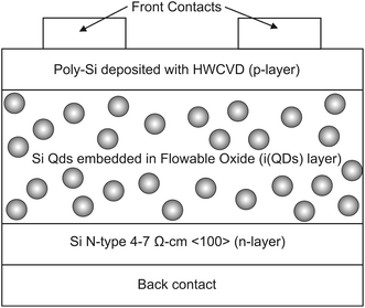
environment at 400 °C for 1 h. Four device structures including n–i, n–p, n–i(QDs) and n–i(QDs)–p were fabricated to study the role of QDs in QDSC. The ‘n–i(QDs)–p’ structure, shown in Fig.
1
, represents QDSC which is studied for current density versus voltage (
J
–
V
) characteristics and external quantum efficiency (EQE) measurement. Capacitance versus voltage (
C
–
V
) measurements are carried out on ‘n–i’ and ‘n–i(QDs)’ structures to study the charge trapping in Si QDs present in ‘i(QDs)’ layers. The
J
–
V
and EQE of a reference device, ‘n–p’ structure, is measured and the performance is compared with QDSC.
Fig. 1
Schematic of Si QDSC ‘n–i(QDs)–p’ structure
Results and discussion
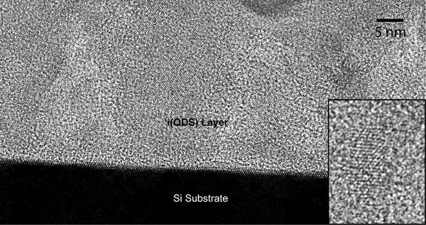
Figure
2
shows cross-sectional high-resolution TEM image of the ‘i(QDS)’ layer and confirms the presence of crystalline Si QDs with particle size (
d
) in the range of 3–8 nm embedded in SiO
2
. The observed particle range represents QDs with energy band gap (
Eg
) in the range of 1.34–2.47 eV as calculated using Eq.
1
[
3
]:
Fig. 2
Cross-sectional high-resolution TEM image of ‘i(QDS)’ layer (thickness ~30 nm) on Si substrate.
Inset
shows an Si QD of 5 nm diameter
EgeV=1.16+11.8d-2.
Si QDs observed are with non-circular shapes and distinct orientation (Fig.
2
) which confirms PS films breakage during sonication to form Si QDs. As measured from high-resolution TEM image, the thickness of the coated ‘i(QDs)’ layer is ~30 nm and the density of the QDs embedded in the layer is 7 × 10
12
#/cm
−2
. The boundaries of the crystallites are ill defined, suggesting surface modification of Si QD. TEM electron diffraction spectra (not shown here) reassert the surface modification of Si QDs. The source of the surface modification is oxidation of particles during sonication [
9
].
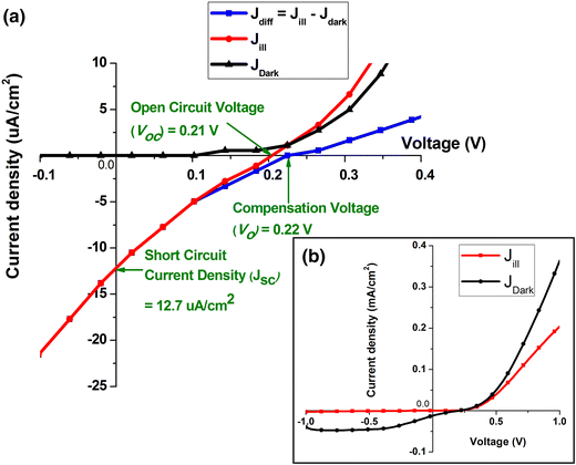
Photovoltaic properties of QDSC with ‘n–i(QDs)–p’ structure are tested under standard test conditions (AM 1.5G spectrum with illumination level equal to 100 mW cm
−2
at 298 K). As shown in Fig.
3
, when illuminated, dark characteristic for QDSC shifts downward confirming the PV properties of the device. QDSC device with area of 1.8 cm
2
shows open circuit voltage (
Voc
) of 0.21 V and short circuit density (
Jsc
) of 12.7 µA cm
−2
. The compensating voltage (
Vo
) for the solar cell, the voltage where
Jdiff
, i.e., difference in
Jill
and
Jdark
becomes zero [
12
,
13
], is 0.22 V. According to [
6
], in QDSC the quasi-Fermi level splits under light illumination, limiting
Voc
of the cell to the band gap of c-Si substrate which is lower as compared to the band gap of Si QDs. Low fill factor (FF) of 21.08 % and the inward bending of illuminated
J
–
V
curve in the fourth quadrant could be partly attributed to quasi-Fermi level splitting. During sonication of PS films, hydrogen and oxygen contaminate Si QDs to produce surface defects [
9
]. Recombination at oxidized QDs surface is also a suggested reason for low values of
Vo
and
Voc
obtained for QDSC [
6
].
Fig. 3
aDark
, photo and illuminated
J
–
V
characteristics of Si QDSC with an area of 1.8 cm
2
measured under standard AM 1.5G spectrum,
binsetJ
–
V
over wide voltage range showing the typical diode-like behavior
To examine the current transport properties of the QDSC, series resistance (
Rs
) of QDSC is estimated from the slope of the linear region of the dark
J
–
V
curve at the forward bias voltages between 0.5 and 1 V. Estimated
Rs
is 1.63 kΩ and such high value of
Rs
limits the fill factor and current output from the device. During
J
–
V
measurements, single aluminum top contact having an area of 1 mm
2
was probed resulting in increased
Rs
decreasing the current collection. To confirm the effect of
Rs
, top Al contacts were changed to finger-type Al contact with a total collection area of 14 mm
2
. With finger-type contact device,
Voc
was 0.21 V,
Jsc
was 0.665 mA cm
−2
, FF was 31.4 % and
Rs
was 31.25 Ω. After increasing the top Al contact area, value of
Rs
was found decreased, resulting in increase of
Jsc
and FF value for the cell. The relation of top contact area and cell performance describe the role
Rs
played in modifying the
J
–
V
curve.
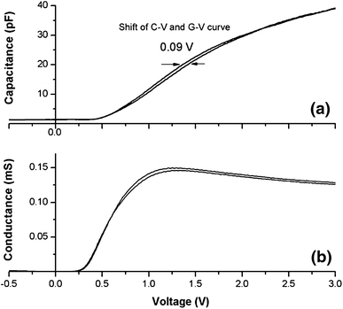
C
–
V
and
G
–
V
characteristics of ‘n–i(QDs)’ structure, measured at 500 kHz and swept from −2 to +2 V, as in Fig.
4
, show the charging effect of the Si nanocrystals embedded in the SiO
2
layer. When subjected to dual voltage sweep, the structure exhibits a hysteresis effect in
C
–
V
characteristics with a voltage shift of 0.09 V. The presence of electron-occupied sites in the ‘n–i(QDs)’ structure produces the hysteresis effect. Since the reference sample with ‘n–i’ structure does not reveal any voltage shift, flowable oxide-turned SiO
2
creates no traps. The source for hysteresis effect is Si QDs with modified surface and QCE due to presence of Si QDs. The peak seen in the
G
–
V
curve appears at the same voltage level where
C
–
V
shows a shift, further confirming the cause of shift to be the presence of Si QDs in the ‘i(QDs) layer. The estimated trap or nanocrystal density using voltage shift with Eq.
2
is 6.43 × 10
11
cm
−2
[
14
].
Dit=Cox/qΔV,
where C
ox
,
q
and
∆V
are oxide capacitance, elementary charge and voltage shift, respectively. The observed voltage shift is, however, small and attributed to the large inter-QD distance or lower QD density in the ‘i(QDs)’ layer. The 1
/C2
behavior of the ‘n–i(QDs)’ structured device, where linear behavior is observed in −0.2 to 0.0 V range, indicating abrupt junction. The built-in voltage of 0.2 V is extracted by extrapolating the straight line to the
x
-axis (Mott–Schottky analysis) [
15
], which is in accordance with the compensation voltage of 0.22 V obtained using
J
–
V
curves.
Fig. 4
C
–
V
and
G
–
V
characteristics of ‘n–i(QDs)’ structure measured at 500 kHz.
Curve
exhibits a shift of 0.09 V on the voltage axis
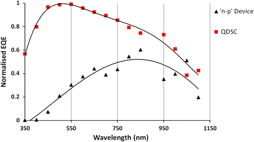
EQE measurement depicts the contribution of Si QDs in the charge collection in the short wavelength of the light. QDSC is subjected to EQE measurement and is compared with reference device having an ‘n–p’ structure. The presence of the ‘i(QDs) layer’ modifies the EQE curve of reference ‘n–p’ device as shown in Fig.
5
. In the short wavelength range (400–550 nm) normalized the EQE plot for QDSC which shows the maximum value. Increased EQE in the shorter-wavelength region is attributed to QCE due to the presence of Si QDs embedded in the ‘i(QDs)’ layer. In the medium- and long-wavelength range, QDSC shows better quantum efficiency as compared to the reference device. SiO
2
present in the ‘i(QDs) layer’ of the device absorbs medium and long wavelength.
Fig. 5
Graph of normalized EQE for Si QDSC and reference ‘n–p’ device
Conclusion
In conclusion, the use of Si QDs synthesized on ultrasonication of freestanding PS films with a top-down approach to fabricate QDSC with ‘n–i(QDs)–p’ structure was successfully demonstrated. Si QDs mixed in flowable oxide was spin coated and then cured to form the Si QD matrix. The best QDSC device showed photovoltaic effect,
Voc
= 0.21 V and
Jsc
= 0.665 mA cm
−2
. It is found that series resistance of the device (
Rs
) controls the current output and FF of the cell. Quasi-Fermi-level splitting and recombination at oxidized Si QDs surface limits
Voc
of the cell. Hysteresis in
C
–
V
characteristics and enhanced EQE performance in the short-wavelength range confirms contribution of QDs toward cell performance.
Authors’ contributions
Dr. PG Kale and Dr. Solanki carried out the study regarding the conceptualisation. Dr. Kale did the design of experiments, carried them out to gather data. He further analysed and interpreted them. Manuscript was drafted by Dr. Kale which was later critically revised by Dr. Solanki.
References
Conniber et al. (2006) Silicon nanostructures for third generation phtovoltaics solar cells (pp. 654-662) 10.1016/j.tsf.2005.12.119
Barth et al. (2010) Synthesis and applications of one-dimensional semiconductors (pp. 563-627) 10.1016/j.pmatsci.2010.02.001
Kim et al. (2004) Quantum confinement effect of silicon nanocrystals in situ grown silicon nitride films (pp. 5355-5357) 10.1063/1.1814429
Shockley and Queisser (1961) Detailed balance limit of efficiency of p-n junction solar cells (pp. 510-520) 10.1063/1.1736034
Yedji et al. (2011) Method for fabricating third generation photovoltaics cells based on Si quantum dots using ion implantation into SiO2 109(8) 10.1063/1.3575325
Di et al. (2011) Improved nanocrystal formation, quantum confinement and carrier transport properties of doped Si quantum dot superlattices for third generation photovoltaics10.1002/pip.1230
Kim et al. (2012) In situ-grown hexagonal silicon nanocrystals in silicon carbide-based films (pp. 634-638) 10.1186/1556-276X-7-634
Unknown ()
Kale et al. (2012) Synthesis and characterization of Si nanoparticles obtained on sonication of porous silicon multilayer films (pp. 13-25) 10.4028/www.scientific.net/JNanoR.17.13
Kale et al. (2012) Investigation of hydrogen storage behavior of silicon nanoparticles 37(4) (pp. 3741-3747) 10.1016/j.ijhydene.2011.04.054
Holzwarth et al. (2007) Optimization of hydrogen silsesquioxane for photonic applications (pp. 2658-2660) 10.1116/1.2787832
Luther et al. (2008) Schottky solar cells based on colloidal nanocrystal films (pp. 3488-3492) 10.1021/nl802476m
Gao et al. (2011) Quantum dot size dependant J–V characteristics in heterojunction ZnO/PbS quantum dot solar cells (pp. 1002-1008) 10.1021/nl103814g
Kim et al. (2001) Ultralarge capacitance-voltage hysteresis and charge retention characteristics in metal oxide semiconductor structure containing nanocrystals deposited by ion-beam-assisted electron beam deposition (pp. 934-937) 10.1063/1.1337618
Park et al. (2009) n-Type silicon quantum dots and p-type crystalline silicon heteroface solar cells (pp. 684-690) 10.1016/j.solmat.2008.09.032