Department of Inorganic Chemistry, Faculty of Chemistry, University of Tabriz, Tabriz, IR
School of Mechanical Engineering WCU Nano Research Center, Yeungnam University, Gyeongsan, 712-749, KR
Laboratory of Photonics and Nano Crystals, School of Engineering-Emerging Technologies, University of Tabriz, Tabriz, IR
Department of Chemistry, Payame Noor University, Tehran, 19395-4697, IR
Faculty of Chemistry, Islamic Azad University, Ardabil, IR
Faculty of Science of Nature, Department of Geology, University of Tabriz, Tabriz, IR
Abstract
Highly crystalline Gd
3+
-doped cadmium oxide micro-structure was synthesized by calcining the obtained precursor of a sol–gel reaction. The reaction was carried out with cadmium nitrate (Cd(NO
3
)
2
·4H
2
O), gadolinium oxide, and ethylene glycol (C
2
H
6
O
2
) reactants without any additives at 80°C for 2 h. The resulting gel was calcined at 900°C with increasing temperature rate of 15°C/min for 12 h in a furnace. As a result of heating, the organic section of the gel was removed, and the Gd
3+
-doped cadmium oxide micro-structure was produced. The obtained compound from the sol–gel technique possesses a cubic crystalline structure at a micro scale. XRD study indicates that the obtained Gd
3+
-doped CdO has a cubic phase. Also, the SEM images showed that the resulting material is composed of particles with cluster structure. Also, FT-IR spectroscopy was employed to characterize the Gd
3+
-doped CdO micro-structures.
Background
Recent research on luminescent nanomaterials provides challenges to both fundamental and breakthrough development of technologies in various areas such as electronics, photonics, display, lasing, detection, optical amplification, and fluorescent sensing in biomedical engineering and environmental control [
1
]. Gadolinium oxide (Gd
2
O
3
) has been frequently used as host material due to abundant resource in nature. Further, Gd is a known contrast agent for magnetic resonance imaging (MRI), and thus the rare-earth ion-doped Gd
2
O
3
can be used in dual, MRI, and fluorescence imaging applications [
2
] and as a drug carrier [
3
]. In addition, pure and doped Gd
2
O
3
films have been studied as high dielectric constant gate dielectric films, phosphor films, and scintillating films [
4
,
5
]. The films of transparent conductive oxides (TCO) such as cadmium oxide (CdO) have been extensively studied because of their use in semiconductor optoelectronic device technology [
6
]. Among the TCO, CdO films have been successfully used for many applications, including use in gas-sensing devices, photodiodes, transparent electrodes, phototransistors, and photovoltaic solar cells [
7
]. Also, CdO is an n-type semiconductor with a cubic crystal structure, possesses a direct band gap of 2.2 eV [
8
]. Besides, CdO shows very high electrical conductivity even without doping due to the existence of shallow donors caused by intrinsic interstitial cadmium atoms and oxygen vacancies [
9
]. In previous studies, the synthesis of Sn-doped CdO thin films [
10
], Bi
3+
-doped CdO thin films by sol–gel spin coating method [
11
], copper-doped CdO nanostructures [
12
], ZnO-doped CdO materials [
13
], titanium-doped CdO thin films [
14
], ZnO-CdO-TeO
2
system doped with the Tb
3+
and Yb
3+
ions [
15
], N-doped CdO [
16
], samarium-, cerium-, europium-, Fe-, and Li-doped CdO nanocrystalline materials [
17
–
21
], In-doped CdO films [
22
], fluorine-doped CdO [
23
], gallium-doped CdO thin films [
24
], Gd-doped CdO thin films with different method, dopant amount and structural morphology [
25
], Li-Ni co-doped CdO thin films [
18
], aluminum-doped CdO thin films [
26
], fluorine-doped CdO Films [
27
] have been reported.
In this work, crystalline Gd
3+
-doped CdO micro-size layer has been synthesized by sol–gel method, with cadmium nitrate (Cd(NO
3
)
2
·4H
2
O), Gd
2
O
3
, and ethylene glycol (C
2
H
6
O
2
) as raw materials without using any catalyst or template at a heat treatment temperature of 900°C with increasing temperature rate of 15°C/min for 12 h, which is a very simple and economical method. Also, we discuss about dopant-concentration effect on the morphology of the synthesized materials. The product was characterized by XRD, SEM, and FT-IR techniques.
Methods
All chemicals were of analytical grade, obtained from commercial sources, and used without further purification. Phase identifications were performed on a powder X-ray diffractometer D5000 (Siemens AG, Munich, Germany) using CuK
α
radiation. The morphology of the obtained materials was examined with a XL30 scanning electron microscope (Philips, Amsterdam, Netherlands). Also, FT-IR spectra were recorded on a Tensor 27 (Bruker Corporation, Germany).
Synthesis of GdxCd1 − xO sub-micron layer (x= 0.02, 0.04, 0.08, and 0.1%)
Cd(NO
3
)
2
·4H
2
O with molar concentrations of 4.83, 4.73, 4.68, and 4.63 mmolar (Mw = 308.482 g mole
−1
), Gd
2
O
3
with molecular concentrations of 0.049, 0.098, 0.0195, and 0.244 mmolar (Mw = 362.5 g mole
−1
), and 10 ml C
2
H
6
O
2
were added into 400 ml distilled water. Then, the solution was stirred at 80°C for 2 h until a dried gel was obtained. The gel was brown color and spongy. The dried obtained gel was treated thermally at 900°C for 12 h. After the reaction was completed and cooled slowly to room temperature, the obtained material was pulverized. The sample was a black-colored powder.
Results and discussion
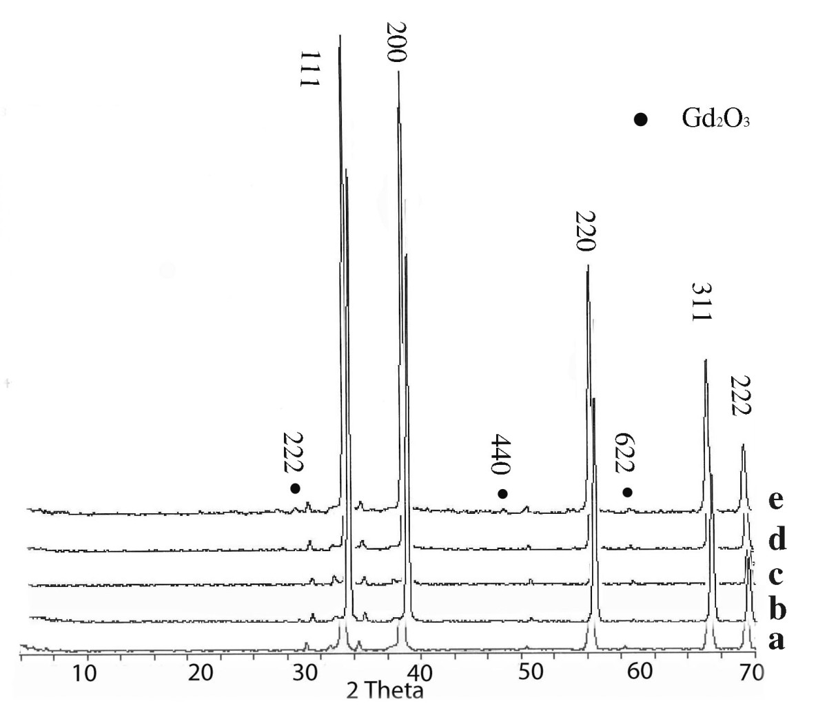
Powder XRD analysis
In order to investigate the structural properties of Gd
3+
-doped CdO micro-structures, X-ray diffraction measurements varying the diffraction angle (with 3° interval) from 4° to 70° were performed. The Gd
3+
-doped CdO diffraction peaks at 2
θ
values of 33.10°, 38.39°, 55.32°, 65.96°, and 69.31° at
x
= 0.08 mmole compared to 2
θ
values of 32.97°, 38.27°, 55.25°, 65.86°, and 69.21° corresponded to pure CdO matching with the 111, 200, 220, 311, and 222 of cubic CdO (JCPDS-05-0640), indicating the formation of CdO- and Gd
3+
-doped CdO with excellent crystallinity. Figure
1
represents the powder XRD (PXRD) patterns of the obtained material after the 12-h reaction time at 900°C and at
xGd
= 0.02, 0.04, 0.08, and 0.1 mmole, respectively. Figure
1
spectrum d shows that increasing the dopant amount to
xGd3+
= 1 mmol, the diffraction peaks at 2
θ
values of 29°, 47°, and 57° match with 222, 440, and 622 assigned to cubic Gd
2
O
3
[
1
–
3
]. So, the doping limitation is
x
= 0 to 0.08 mmole. Crystal sizes were measured via Debye-Scherrer's equations, which are as follows: 29.0, 27.8, and 27.65 nm for
x
= 0.02, 0.04, and 0.08 mmole dopant concentration, respectively. Also, the interplanar spacing in the crystalline material is calculated via Bragg's law (
nλ
= 2
dhkl
sin
θ
) selecting the peaks
h
,
k
, and
l
at 200. The radius of Gd
3+
(
r
= 0.94 Å [
28
]) is smaller than the radius of Cd
2+
(
r
= 1.1 [
28
] Å); compared to those of the pure particles, the diffraction lines in the powder XRD patterns of Gd
3+
-doped CdO shift to higher 2
θ
in doped CdO. So, we have the following equations:
Δ
2
θ
= 38.39 (doped) − 38.27 (pure) = 0.12° and
Δd
= 2.34903 (pure) − 2.34196 (doped) = 0.00707 Å. The shift in the diffraction lines might be attributed to the smaller radius of the dopant ion, compared to the ionic radius of the Cd
2+
, which may cause a contraction of the unit cell and so decrease the lattice parameters in the Gd
3+
-doped CdO materials. The pattern shows the polycrystalline of cubic CdO structure (NaCl structure of a space group
Fm3m
). According to JCPDS-05-0640, the lattice constants for an undoped CdO sample were
a
= 0.46950 nm. Also, we used CelRef software version 3, using XRD patterns 2
θ
and
h
,
k
, and
l
values, to refine the cell parameters. Pure CdO cell parameters calculated as
a
= 0.46941 nm and for doped CdO (in
x
= 0.08 mmole) were
a
= 0.46912 nm. The calculations showed that the unit cell volume of pure CdO is 0.1034 nm
3
and that of the doped CdO is 0.10324 nm
3
. So, we can conclude that there is a contraction in the unit cell when doping Gd
3+
in CdO. The PXRD measurements confirm that a pure phase of the cubic CdO is formed [
28
–
34
].
Figure 1
PXRD patterns of the synthesized pure CdO and GdxCd1 −xO micro-material.(a)
Pure CdO,
(b)x
= 0.02,
(c)x
= 0.04,
(d)x
= 0.08, and
(e)x
= 0.1 mmole.
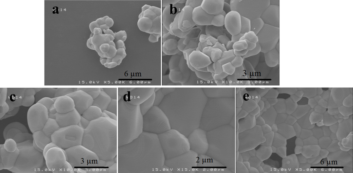
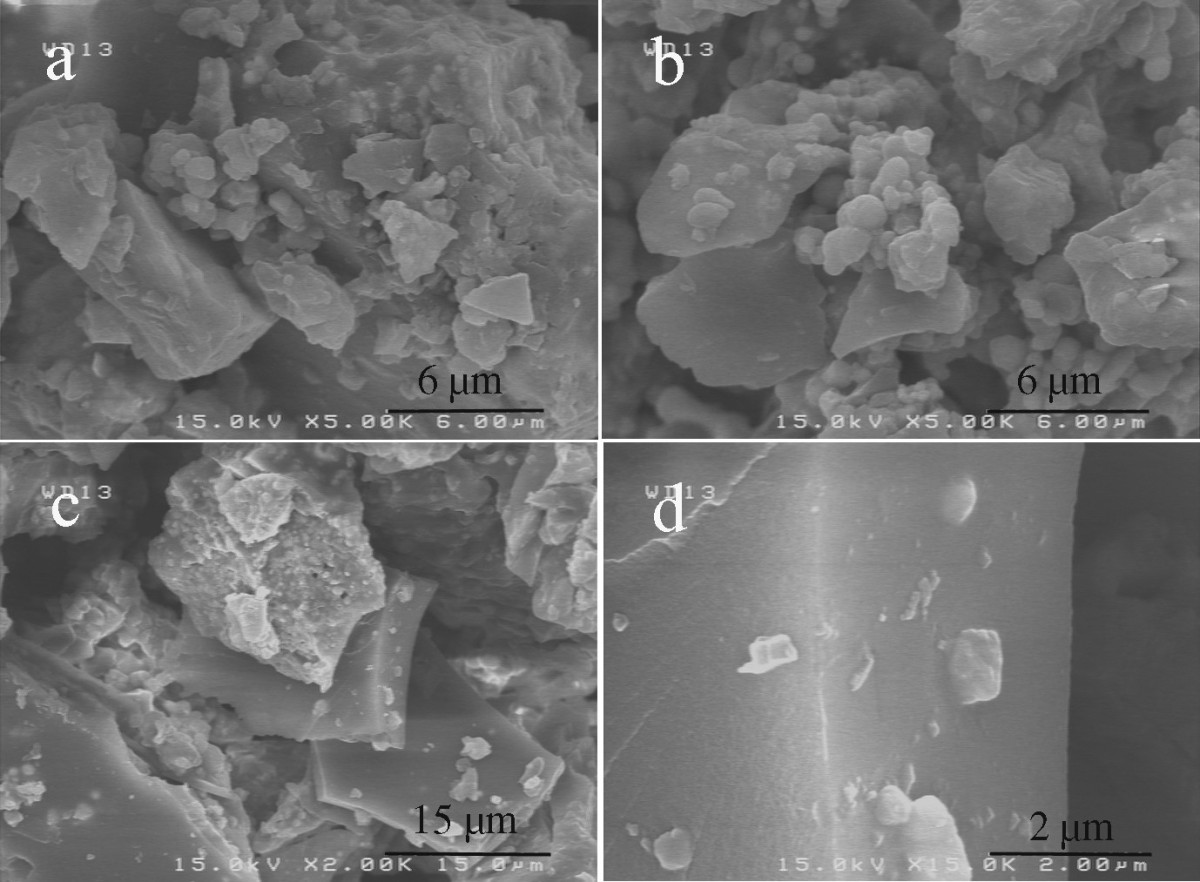
Micro-structure analysis
Figure
2
reveals the SEM images of the cubic structure of the obtained crystalline CdO at 900°C [
33
]. Remarkably, it was observed that the average particle size is 2 μm. As shown in Figure
2
a,b, it is clear that the material is composed of particles with heterogeneous size. Figure
2
c shows that the sample is nearly a layer-like structure with macro-pores which resulted from the calcination treatment. Figure
2
d,e shows that the morphology is clearly like a layer, with the particle almost spherical in shape and size in a range of about 2 to 3 μm. SEM images in Figures
3
,
4
, and
5
reveal the general morphological aspect of the powder particles. SEM images of the synthesized Gd
3+
-doped CdO sub-micron materials are presented in Figure
3
,
4
, and
5
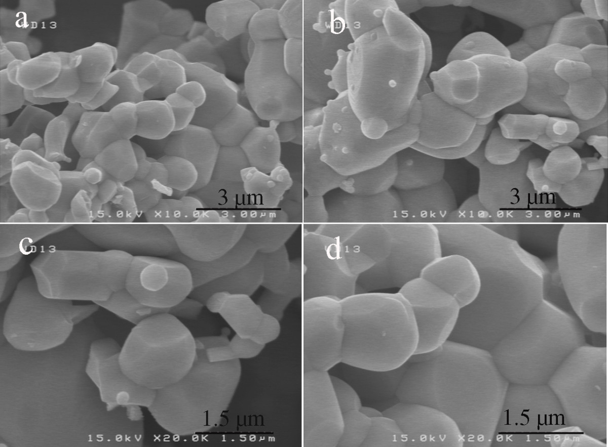
. Figure
3
shows the SEM images of Gd
0.02
Cd
0.98
O sub-micron particle. The synthesis of the sol–gel system led to the formation of spheroidal-shaped particle clusters. As shown in Figure
3
a,b, with low magnification, the sample is like a macro-porous structure, and it is clear that the particle sizes that formed the structure are heterogonous. With high magnification, this figure shows that there are small particles (uncus) on the surface of the particles. The average uncus particle size was estimated between 200 and 300 nm. With higher magnification, Figure
3
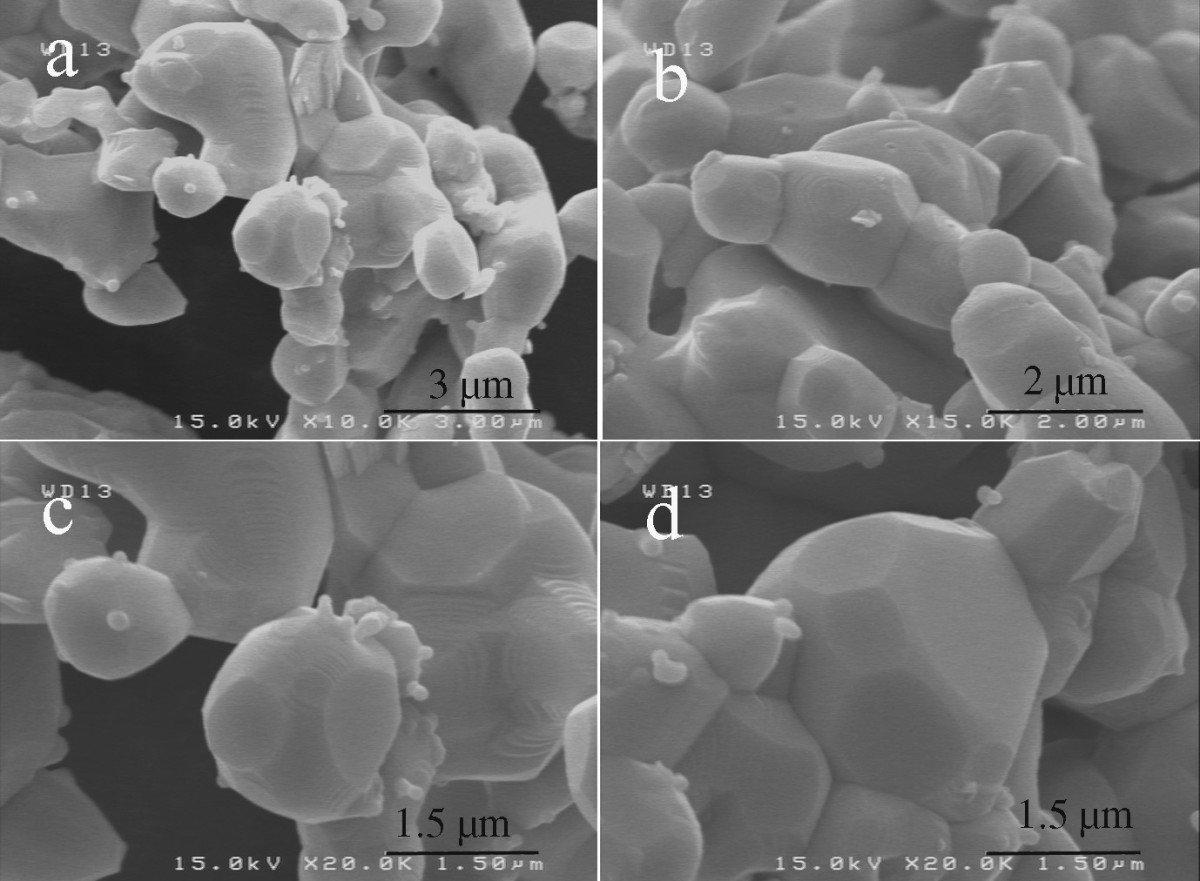
c,d shows that the multigonal particle sizes are about 1 μm. Compared to pure CdO, it seems that the morphology of the particles is changed from layer-like to macro-porous particles. Figure
4
a,b shows Gd
0.04
Cd
0.96
O; due to increasing dopant concentration, the number of uncus particles is increased. The uncus sizes are a little smaller than those of Gd
0.02
Cd
0.98
O sub-micron particle. In Figure
4
c,d, it is clear that with increasing dopant concentration, the morphology of the synthesized materials is almost unchanged. Figure
5
a,b shows Gd
0.08
Cd
0.92
O; due to increasing dopant concentration, the morphology of the particles was changed to a layer-like structure. Also, in Figure
5
c,d, it is clear that there are particles with spheroid structure. The particle sizes are heterogeneous and about 1 μm. In Figure
5
d, it is clear that the width of the layer structure is about 3 μm. This Figure shows that there are small particles on the surface of the layer as uncus. The uncus particle sizes are heterogeneous and are estimated to be between 100 and 500 nm; considering the smallest uncus particle (100 nm), the uncus particles in Figure
5
are smaller than those of Gd
0.04
Cd
0.96
O.
Figure 2
The SEM images of the synthesized CdO sub-micron materials.(a, b)
SEM image of pure CdO the material is composed of particles with heterogeneous size.
(c)
The sample is nearly a layer-like structure.
(d)
The morphology is clearly like a layer with macro-pores, with the particle almost spherical in shape and size in a range of about 2 to 3 μm.
Figure 3
The SEM images of the synthesized Gd0.02Cd0.98O sub-micron materials.(a, b)
the sample is like a macro-porous. Structure and there are small particles (uncus) on the surface of the particles.
(c, d)
the multigonal particle sizes are about 1 μm. And the morphology of the particles is changed from layer-like to macro-porous particles.
Figure 4
The SEM images of the synthesized Gd0.04Cd0.96O sub-micron materials.(a, b)
due to increasing dopant concentration, the number of uncus particles is increased.
(c, d)
that with increasing dopant concentration, the morphology of the synthesized materials is almost unchanged.
Figure 5
The SEM images of the synthesized Gd0.08Cd0.92O sub-micron materials.(a, b)
the particles was changed to a layer-like structure.
(c, d)
there are particles with spheroid structure. The particle sizes are heterogeneous and about 1 μm. And there are small particles on the surface of the layer as uncus.
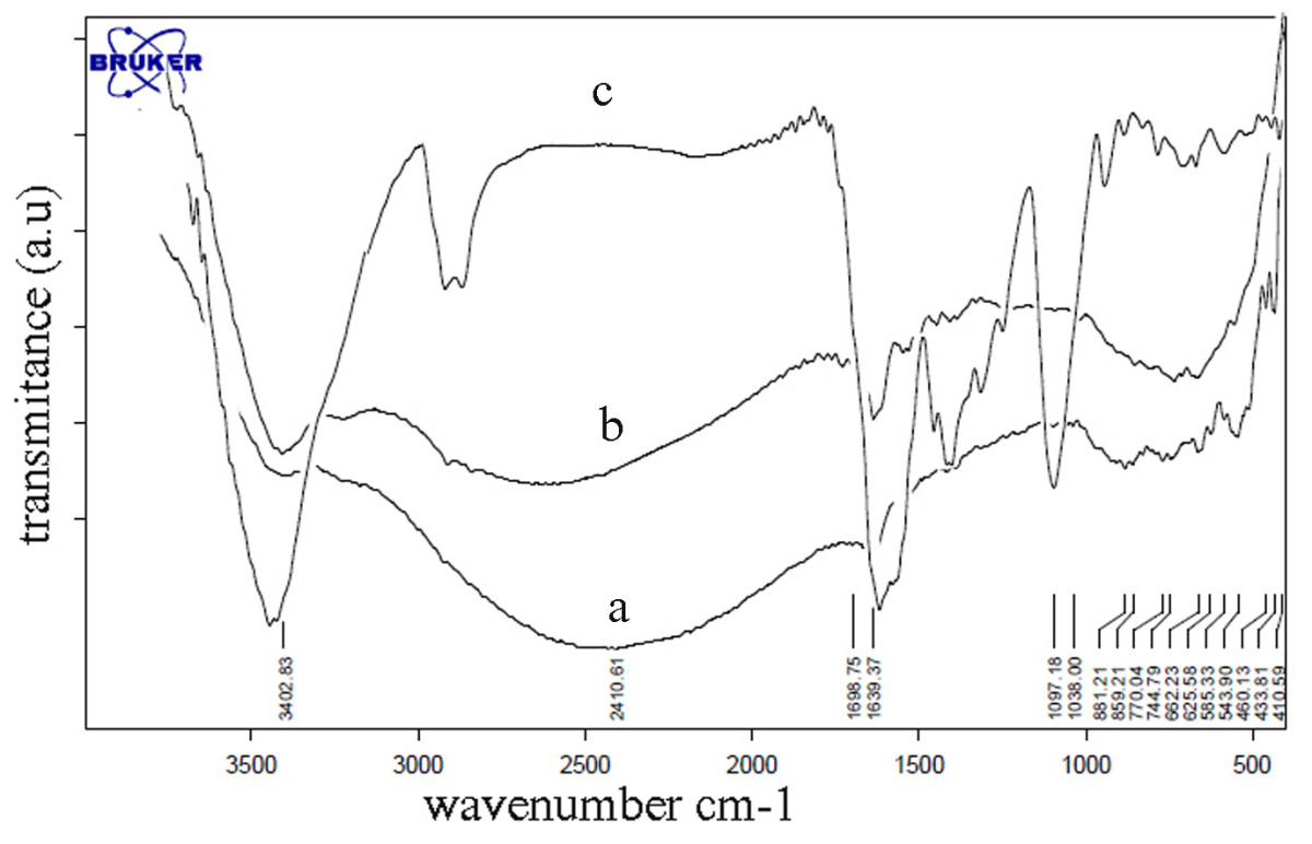
Spectroscopic study
Figure
6
shows the FT-IR spectrum diagram of the doped samples. The bands around 3,460 and 1,650 cm
−1
are due to the OH stretching vibration and OH deformation vibration, respectively. The absorption appearing around 1,510 and 1,410 cm
−1
corresponds to CO asymmetric vibration. The band at 540 cm
−1
is assigned to the Gd-O vibration mode of the cubic Gd
2
O
3
[
3
]. Also, we know that the peaks at 800 to 1,400 are assigned to CdO [
35
]. Peak at 1,541 cm
−1
corresponded to the residual organic components [
36
].
Figure 6
FT-IR spectra of the synthesized GdxCd1 −xO sub-micron materials.(a)x
= 0.02,
(b)x
= 0.04,
(c)x
= 0.08 mmole obtained after 12 h at 900°C.
Conclusion
In summary, micro-layers of Gd
3+
-doped CdO were synthesized successfully by employing a simple sol–gel method. We found that the dopant concentration affects the morphology of the final product. As shown by the SEM images, with increasing dopant concentration, the morphology of the cluster-like micro-crystals changed to partially layered structures. We found that compared to those of the micro-size material of pure CdO, the diffraction lines in the powder XRD patterns of Gd
3+
-doped CdO shifted to higher 2
θ
values. The shift in the diffraction lines might be attributed to the smaller radius of the dopant ion, compared to the ionic radius of the Cd
2+
, which may cause a contraction of the unit cell and so decrease the lattice parameters in the Gd
3+
-doped CdO materials. These materials are expected to have a potential application in dual, MRI, and fluorescence imaging applications and as a drug carrier.
Authors' information
SK got his B.S. degree in Applied Chemistry from the University of Birjand in 2007. He got his M.Sc. degree in Inorganic Chemistry from the University of Tabriz in August 2010. He is now finishing his Ph.D. studies in Inorganic Chemistry in the Faculty of Chemistry of the University of Semnan, Iran. AA got his B.S. and M.Sc. degrees in Chemistry from the University of Tabriz, Iran in 1972 and 1974, respectively. He got his Ph.D. degree in Inorganic Chemistry from the University of Paris, France in 1978. He is now a professor in Inorganic Chemistry at the University of Tabriz, Iran. MD got his B.S. and M.Sc. degrees in Chemistry and in Inorganic Chemistry from the University of Tabriz, Iran in 2004 and 2006, respectively. He got his Ph.D. degree in Inorganic-Solid State Chemistry from the University of Tabriz, Iran in 2010. She is now a postdoctorate student and associate professor in the research group of Prof. Rostami at the School of Engineering Emerging Technologies, University of Tabriz, Iran and in the Department of Inorganic Chemistry in the same university. AB got his B.S. and M.Sc. degrees in Chemistry and in Inorganic Chemistry from the University of Tabriz, Iran and from the University of Urmia in 2004 and 2006, respectively. He got his Ph.D. degree in Inorganic Chemistry from University of Tabriz, Iran in 2010. He is now an associate professor in the University of Payamenoor, Tehran. HM is now a M.Sc. student in Inorganic Chemistry in Azad University (Ardabil branch). SS is now a Ph.D. student in Faculty of Science of Nature at University of Tabriz.
Acknowledgments
The authors express their sincere thanks to the authorities of Tabriz University for financing the project.
Competing interest
The authors declare that they have no competing interests.
Authors' contributions
All authors (AA, SK, SWJ, MD, AB, HM, and SS) participated in the experiments and read and approved the final manuscript.
References
Jayasimhadri et al. (2010) Conversion of green emission into white light in Gd2O3 nanophosphors10.1016/j.tsf.2010.03.173
Liu et al. (2008) Enhanced photoluminescence of Sm3+/Bi3+ co-doped Gd2O3 phosphors by combustion synthesis10.1016/j.jlumin.2008.06.013
Chang et al. (2010) Synthesis and characterization of mesoporous Gd2O3 nanotube and its use as a drug-carrying vehicle10.1016/j.actbio.2010.03.009
Guo et al. (2004) Structure and optical properties of sol–gel derived Gd2O3 waveguide films10.1016/j.apsusc.2004.02.032
Hussein (1994) Formation, characterization, and catalytic activity of gadolinium oxide. Infrared spectroscopic studies10.1021/j100089a047
Haul and Just (1962) Disorder and oxygen transport in cadmium oxide10.1063/1.1777147
Zheng et al. (2011) Optical and electrical properties of Sn-doped CdO thin films obtained by pulse laser deposition10.1016/j.vacuum.2011.01.002
Dagdelen et al. (2012) Preparation of nanostructured Bi-doped CdO thin films by sol–gel spin coating method10.1016/j.matlet.2012.04.087
Benhaliliba et al. (2012) Luminescence and physical properties of copper-doped CdO derived nanostructures10.1016/j.jlumin.2012.03.044
Kavasoglu et al. (2009) Observation of negative photoconductivity in (ZnO)x(CdO)1 − x films10.1016/j.jpcs.2008.11.018
Gupta et al. (2008) Effect of oxygen partial pressure on structural, optical and electrical properties of titanium-doped CdO thin films10.1016/j.apsusc.2008.07.102
Ruvalcaba-Cornejo et al. (2008) Photoluminescence properties of the ZnO–CdO–TeO2 system doped with the Tb3+and Yb3+ ions10.1016/j.jlumin.2007.07.004
Dakhel (2011) Effect of thermal annealing in different gas atmospheres on the structural, optical, and electrical properties of Li-doped CdO nanocrystalline films10.1016/j.solidstatesciences.2011.02.002
Dakhel (2009) Influence of annealing in nitrogen on the structural, electrical, and optical properties of CdO films doped with samarium10.1016/j.matchemphys.2009.06.003
Dakhel (2011) Effect of cerium doping on the structural and optoelectrical properties of CdO nanocrystallite thin films10.1016/j.matchemphys.2011.06.060
Salih et al. (2009) In doped CdO films: electrical, optical, structural and surface properties10.1016/j.ijhydene.2008.11.110
Metin et al. (2007) Electrical and optical properties of fluorine-doped CdO films deposited by ultrasonic spray pyrolysis10.1016/j.solmat.2007.01.020
Deokate et al. (2010) Structural, optical and electrical properties of chemically sprayed nanosized gallium doped CdO thin films10.1016/j.jallcom.2010.01.150
Gupta et al. (2011) Low temperature processed highly conducting, transparent, and wide bandgap Gd doped CdO thin films for transparent electronics10.1016/j.jallcom.2011.01.007
Gupta et al. (2012) Bandgap variation in size controlled nanostructured Li–Ni co-doped CdO thin films10.1016/j.jallcom.2011.11.098
Maity and Chattopadhyay (2006) Synthesis and characterization of aluminum-doped CdO thin films by sol–gel process10.1016/j.solmat.2005.05.001
Seval et al. (2009) Effect of heat treatment on physical properties of CdO films deposited by sol–gel method10.1016/j.ijhydene.2008.09.057
Vigil et al. (2001) Structural and optical properties of annealed CdO thin films prepared by spray pyrolysis10.1016/S0254-0584(00)00358-8
Dakhel (2008) Influence of hydrogenation on the electrical and optical properties of CdO:Tl thin films10.1016/j.tsf.2008.08.114
Alemi and Khademinia (2013) Sol–gel synthesis, characterization and optical properties of CdO micro-size materials
Yakuphanoglu et al. (2010) Electrical characterization of nanocluster n-CdO/p-Si heterojunction diode10.1016/j.jallcom.2010.06.174
Askarinejad and Morsali (2008) Syntheses and characterization of CdCO3 and CdO nanoparticles by using a sonochemical method10.1016/j.matlet.2007.05.082
Tadjarodi and Imani (2011) Synthesis and characterization of CdO nanocrystalline structure by mechanochemical method10.1016/j.matlet.2010.12.054