Methods
Discretization of Maxwell’s equations
The structure under our consideration is a PC system consisting of periodic dielectric rods with finite thickness in a two-dimensional slab. Figure
1
a shows a PC slab sandwiched between two high-dielectric-constant layers parallel to the
x
-axis direction. Also, due to total reflection, the electric field vanishes at the boundaries. Although the slab is limited in width, the
x
-axis direction is unlimited. A point defect can be easily exhibited by inserting an air rod instead of one of the dielectric lattice sites (Figure
1
b) while the nearest neighboring dielectric rods are numbered. We begin our investigation by following Maxwell’s equations for electric field
E
and magnetic field
H
:
A PC slab.
A PC slab consisting of high-dielectric rods between low-dielectric background which is sandwiched in two high-dielectric-constant layers parallel to the
x
-axis direction, (
a
) the perfect system and (
b
) the imperfect system, while the central rod is removed. The neighboring sites are not removed but are indicated by numbers.Figure 1

where
ω
is the light frequency,
c
is the light velocity, and
ε
r
(
r
) is the dielectric constant. By assuming that the dielectric constant
ε
r
(
r
) is independent of the
z
coordinate, we rewrite the first equation for a two-dimensional slab. We just study the TM mode since the mentioned PC structure with dielectric rods is appropriate for TM modes [
19
,
20
]. This formalism is general, and for TE modes the same procedures have to be reviewed. Extending the method implemented in [
12
], we discretize Equation
1
since for TM modes the main components of fields are (
E
z
,
H
x
,
H
y
); therefore, the electric field and the other two components can be solved by the following differential equations:
The corresponding equation for
E
z
in the form of operator equation with a Hermitian differential operator could be defined as [
12
]
where
L
and the function
f
for TM modes are defined by
This equation has to be discretized in the
x
direction, and the position of the center of the
l
th site in the
x
direction is indicated by
x
l
=
l
a
0
and in the
y
direction by
y
α
=
α
a
0
, where
a
0
is the lattice constant and
l
and
α
are integers. While
l
is an infinite number,
α
is finite. By using the following discretization of Equation
5
,
where
where the coefficients are defined as
General form of tight binding model for a PC slab
For mapping of light propagation in a PC to a tight binding model, we introduce photon creation and annihilation operators
When the Hermitian operator
where
where ∣0> is the photonic vacuum state. The result is equivalent to the finite differential equation (
7
). To distinguish defected and perfect systems, index zero is used for the perfect system. Equation
11
, in terms of perfect system operators and onsite and hopping energies, is given by
where prime
The matrix element of Equation
14
is
where
Now an efficient propagator, the Green function [
21
], is defined:
In the following part, we determine the Green functions for the described system to calculate the defected slab electric field.
PC slab Green function
According to Equation
10
, we act the operator
then the Green function is defined:
The field stateket ∣
f
> or the electric field ket can be determined according to [
20
], but since the electric field vanishes at the limited boundaries, the following relation is adequate for the electric field stateket:
where
A 1D Bravias lattice site.
Mapping of a PC slab to a 1D Bravias lattice site is shown schematically. The horizontal axis is infinite, while the vertical axis is finite.Figure 2

therefore, a general relation for the perfect slab Green function component is
however, for the case of the electric ket Equation
19
, we have a simpler form of this component:
This Green function, is used to relate that defected system field to the perfect system field by the Lippmann-Schwinger formalism.
Lippmann-Schwinger equation
The electric field component in the
z
-axis direction,
inserting Equation
19
, we have
Perturbation modifies the electric field, but with first-order approximation of the Lippmann-Schwinger formalism, we relate the defected system electric field to perfect system’s. For this purpose, we write
Using
where the right-hand side of Equation
25
is equal to
G
0
−1
ψ
l
; then, all ends to the Lippmann-Schwinger equation:
For calculating
G
0
, we should have the proper dispersion relation of the slab that is illustrated in Figure
1
. Therefore, by Equations
7
and
19
and some mathematics, we obtain the desired relation:
which is based on tight binding method and is applicable only for the described slab.
Application of the method to a PC slab
In order to relate the wave function of a defected system to a perfect system, Equation
26
is rewritten while a perturbation term is included:
We apply this model for a quasi-one-dimensional PC slab consisting of periodic dielectric rods in which the dielectric constant
ε
r
=8.9 and the central defect site is an air cylinder with a circle cross section. The slab is infinite along the
x
direction, but due to layering high-dielectric-constant material sheets on its borders parallel to the
x
direction, it has a finite
y
direction. Although we have considered the first neighboring sites, the difference of the dielectric constant term for neighboring sites,
The dispersion relations for different integer numbers.
Dispersion relation in terms of
k
x
is plotted for two different numerical integers of
ν
corresponding to
The ratio of electric field for defect site.
The ratio of electric field with respect to its clean system at defect site
l
=0 in sub-site
α
=3 (central site) is plotted. The peak’s height is maximum 10.2 at frequency 0.819 corresponding to the edges of the first BZ (the third axis). The ratio of field intensity at defect site.
The ratio of electric field intensity with respect to its clean system at defect site is plotted. The peak’s height is maximum 103 at frequency 0.819. The ratio of field intensity for the first neighboring site of right/left side of defect site.
The ratio of field intensity with respect to its clean system for the site
l
=±1 and sub-site
α
=3 (right side or left side of the defect site) is presented. The peak’s height is maximum 10.0, with
The field intensity for defect site.
The ratio of electric field intensity with respect to its clean system at defect site, corresponding to
ν
=1,2,3,4,5 of Figure
3
b. The peak’s height is maximum 17,100, with
A comparison of electric fields for different sites.
The ratio of electric field of defect site (black line) and the first neighboring site on right or left side of the defect (yellow line) are compared which indicates similarity at lower frequencies but difference at higher frequencies.
k
x
is constant corresponding to the first BZ edge. A comparison of the ratio of field intensity for different sites.
The ratio of electric field intensity of defect site (black line) and the first neighboring site on the right or left side of the defect (yellow line) are compared which indicates that the maximum field intensity of the neighboring site is at higher frequency.
k
x
is constant corresponding to the first BZ edge. A comparison of electric fields for different sites.
The ratio of electric field of defect site (black line) and the first neighboring site on upside or downside of the defect (green line) are compared which indicates different signs of electric field for all range of frequency.
k
x
is constant corresponding to the first BZ edge. A comparison of the ratio of field intensity for different sites.
The ratio of electric field intensity of defect site (black line) and the first neighboring site on upside or downside of the defect (green line) are compared which indicates that the maximum field intensity of the neighboring site and defect site are at the same frequency.
k
x
is constant corresponding to the first BZ edge. A comparison of electric fields for different sites.
The similarities and differences of the sign and amount of the electric field at three sites are compared: the first neighboring site of the right or left (yellow line), the first neighboring site on upside or downside of the defect (green line), and the second neighboring site on each corner side of the defect (dark blue line).
k
x
is constant corresponding to the first BZ edge. A comparison of the ratio of field intensity for different sites.
The ratio of electric field intensity of the first neighboring site of the right or left (yellow line), the first neighboring site on upside or downside of the defect (green line), and the second neighboring site on each corner side of the defect (dark blue line) is compared.
k
x
is constant corresponding to the first BZ edge.Figure 3
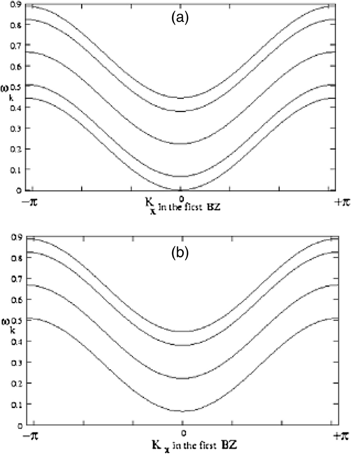
Figure 4
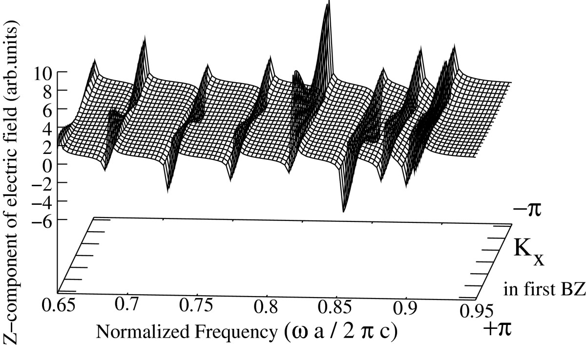
Figure 5

Figure 6
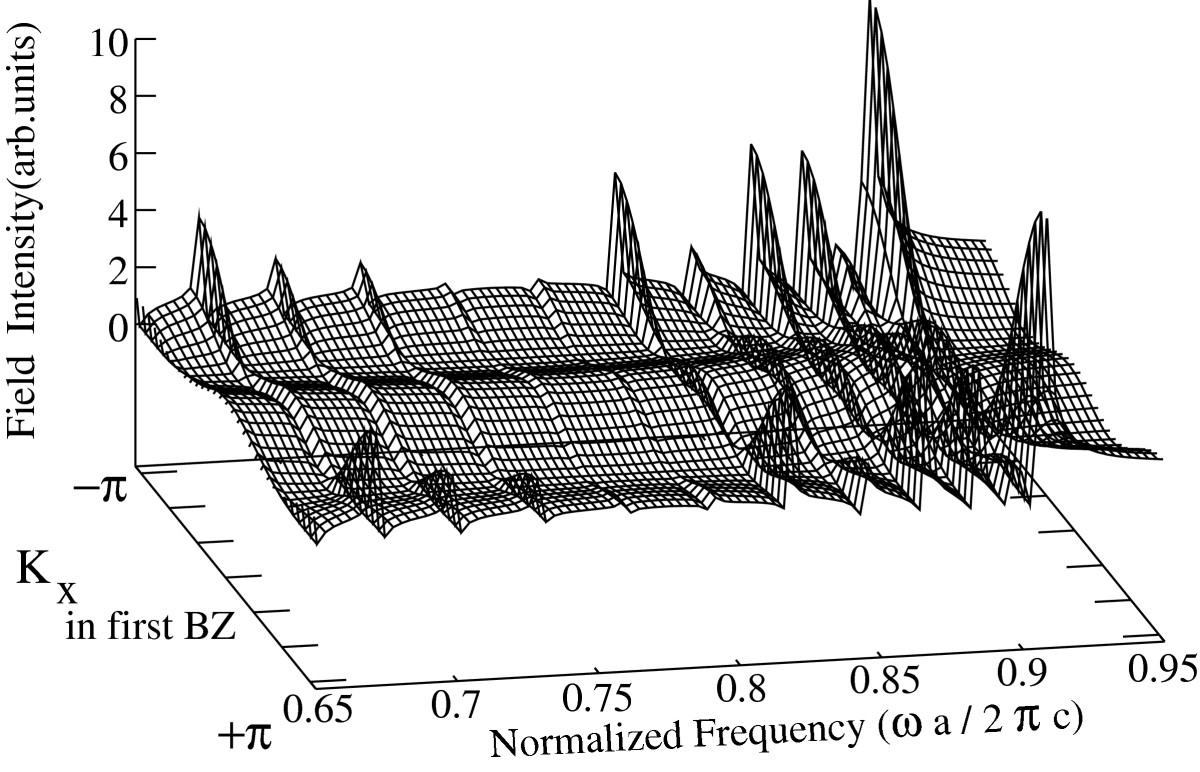
Figure 7

Figure 8

Figure 9

Figure 10

Figure 11

Figure 12

Figure 13
