Results and discussion
PXRD analysis
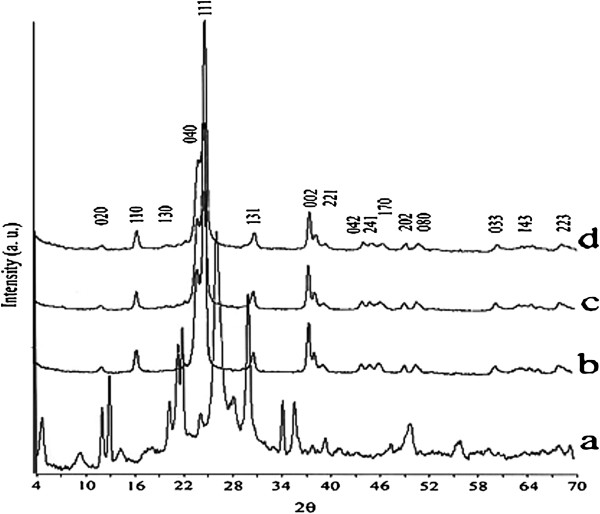
Figure
1
represents the PXRD patterns of the obtained Li
2
SiO
3
nanomaterials after reaction times of 48, 72, and 96 h. The PXRD measurements confirm that when the Li/Si molar ratio in the reaction mixture is 1:2, a pure phase of the orthorhombic Li
2
SiO
3
(space group of
Cmc
2
1
[
29
–
35
]) is formed. In contrast, as shown in Figure
2
, with the Li/Si molar ratio of 1:3 in the reaction mixture, a mixture of meta-stable Li
2
Si
2
O
5
(space group of
Pbcn
[
36
,
37
]) and Li
2
SiO
3
is obtained after 48 h. By increasing the reaction time to 72, 96, or 120 h, a pure highly crystalline phase of meta-stable Li
2
Si
2
O
5
is obtained. A stable form of this compound crystallizes in the space group of
Ccc
2 [
38
]. However, most papers refer to a monoclinic cell [
19
,
39
–
43
] despite noticing a discrepancy in diffraction peak intensities between the experiment and calculation. The monoclinic cell has a different symmetry but the same size as the
Ccc
2 stable form (
β
= 90°) [
44
]. Particle sizes that were measured via Debye-Sherrer equation are as follows: Lithium metasilicate particle sizes are 26.12, 26.82, and 24.58 nm for 48, 72, and 96 h reaction times, respectively. Lithium disilicate particle sizes are 20.696, 22.50, and 23.86 nm for 72, 96, and 120 h reaction times, respectively. Also, interplanar spacing in the crystalline material are calculated via Bragg’s law (
n
λ = 2d
hkl
sin
θ
)). Thus compared to those of the nanoparticles of pure lithium silicates, with increasing the reaction time, the diffraction lines in the powder XRD patterns of the nanoparticles of lithium metasilicates shift to higher 2
θ
values (
Δ
2
θ
= 26.84(48 h) - 26.88(96 h) = 0.04° and Δd = 3.3177 Å (48 h) - 3.3128 Å (96 h) = 0.0049 Å; and with increasing the reaction time, the diffraction lines in the powder XRD patterns of the nanoparticles of lithium disilicates shift to lower 2
θ
values Δ2
θ
= 30.66(72 h) - 30.59(120 h) = 0.07°, Δd = 2.9190 Å (120 h) - 2.9125 Å (72 h) = 0.065 Å. According to above measurements, particle sizes measured with Debye-Sherrer equation are in good agreement with interplanar spacing in the crystalline material measured via Bragg’s law.
PXRD patterns of the synthesized Li
2
SiO
3
nanomaterials after different times at 180
°C
.
(
a
) 48, (
b
) 72, and (
c
) 96 h. PXRD patterns of the synthesized Li
2
Si
2
O
5
nanomaterials after different times at 180
°C.
(
a
) 48, (
b
) 72, (
c
) 96, and (
d
) 120 h.Figure 1
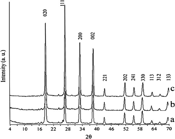
Figure 2
Microstructure analysis
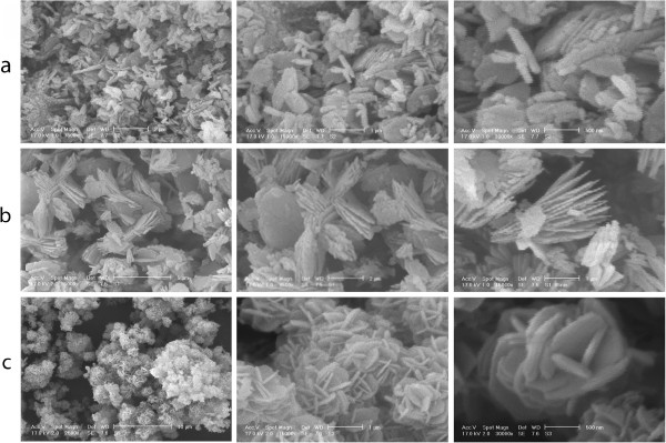
The SEM images of the synthesized Li
2
SiO
3
nanomaterials are given in Figure
3
. With the reaction time of 48 h, ununiform sheet-like nanoparticles of Li
2
SiO
3
are obtained (Figure
3
a). The thicknesses, widths, and lengths of the resultant sheets are approximately 100 nm, 600 nm and 2 μm, respectively. With increasing the reaction time to 72 h, the morphology of the obtained materials has been changed to the very compact sheets with heterogeneous morphology (Figure
3
b). This is while with the reaction time of 96 h, uniform flower-like nanoparticles are obtained (Figure
3
c).
The SEM images of the synthesized Li
2
SiO
3
nanomaterials obtained after different times at 180
°C.
(
a
) 48, (
b
) 72, and (
c
) 96 h.Figure 3
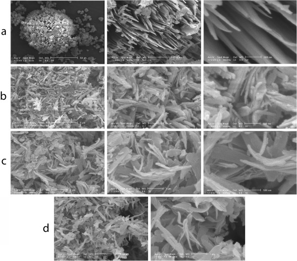
Figure
4
represents the SEM images of the synthesized Li
2
Si
2
O
5
nanomaterials. After 48 h, the morphology of the obtained material is sponge-like, consisting of sheet-like and flower-like nanoparticles (Figure
4
a). With increasing the reaction time to 72, 96, and 120 h, the morphology of the obtained materials has been changed to the rectangular sheets and high homogeny in the size is achieved. According to Figure
3
with image magnification of 15,000, it is clear that with increasing reaction time, the grain size has been decreased. Moreover, according to Figure
4
, with image magnification of 15,000, it is clear that with increasing the reaction time the grain size has been increased. So Figures
3
and
4
are in agreement with the calculated particle size and interplanar spacing in the crystalline material measured in PXRD analysis section.
The SEM images of the synthesized Li
2
Si
2
O
5
nanomaterials obtained after different times at 180
°C.
(
a
) 48, (
b
) 72, (
c
) 96, and (
d
) 120 h.Figure 4
Spectroscopic studies
The electronic absorption spectra and also the emission spectra of the synthesized Li
2
SiO
3
and Li
2
Si
2
O
5
nanomaterials are given in Figures
5
and
6
, respectively. An intense absorption band at 276, 275, and 275 nm is observed in the electronic absorption spectra of the Li
2
SiO
3
nanomaterials obtained after 48, 72, and 96 h at 180°C respectively. A similar intense absorption band is observed at 272, 274, and 277 nm in the electronic absorption spectra of the Li
2
Si
2
O
5
nanomaterials obtained after 48, 72, and 96 h at 180°C, respectively.
Electronic absorption spectra of Li
2
SiO
3
and Li
2
Si
2
O
5
obtained after 96 h at 180
°C.
The electronic absorption spectra of the synthesized Li
2
SiO
3
(
a
) and Li
2
Si
2
O
5
(
b
) nanomaterials obtained after 96 h at 180°C. Emission spectra of Li
2
SiO
3
and Li
2
Si
2
O
5
obtained after 96 h at 180
°C.
The emission spectra of the synthesized Li
2
SiO
3
(
a
) and Li
2
Si
2
O
5
(
b
) nanomaterials obtained after 96 h at 180°C.Figure 5
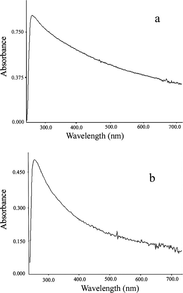
Figure 6
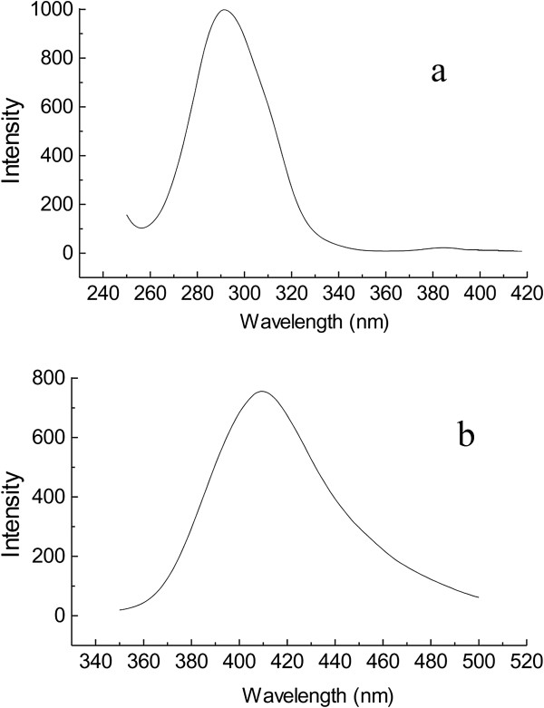
In the excitation spectrum of the synthesized Li 2 SiO 3 and Li 2 Si 2 O 5 nanomaterials, a band is observed with maxima at 360 and 250 nm, respectively. Accordingly, in the emission spectrum of the synthesized Li 2 SiO 3 nanomaterials, an intense peak appears at 410.03 nm. In comparison, an intense peak at 291.45 nm is observed in the emission spectrum of the synthesized Li 2 Si 2 O 5 nanomaterials. With increasing in the reaction time, no shift is observed in the emission spectrum of the obtained Li 2 SiO 3 and Li 2 Si 2 O 5 nanomaterials. However, increasing band intensities in the emission spectra of both compounds are observed with increasing reaction time.
Structural optimization
The crystal structure and locations of the atoms of the Li 2 SiO 3 [ 45 ] and Li 2 Si 2 O 5 [ 36 ] determined from X-ray diffraction data are used as a starting point for total energy minimization. The optimized unit cells of the Li 2 SiO 3 and Li 2 Si 2 O 5 are shown in Figures 3 and 4 , respectively. Optimization (relaxation) of the atomic positions and crystal cell parameters was performed before the main calculations of the electronic characteristics, total electronic energy, band energy dispersion, density of electronic states, and optical properties.
Electronic structures
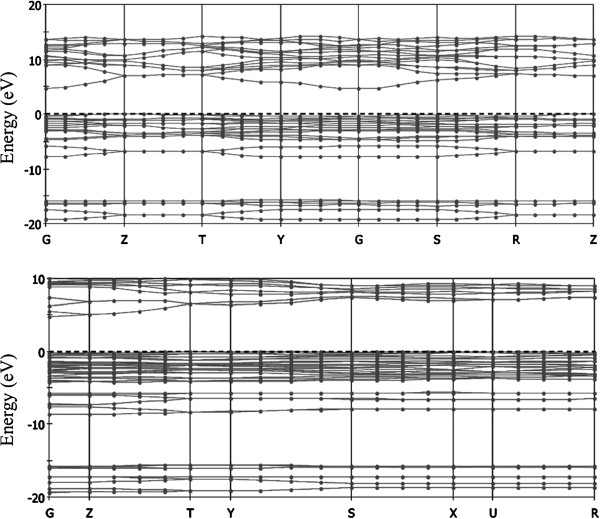
The calculated band structure of the compounds along high symmetry points of the first Brillouin zone is plotted in Figure
7
, where the labeled
k
points are present as G (0.000, 0.000, 0.000), Z (0.000, 0.000, 0.500), T (-0.500, 0.500, 0.500), Y (-0.500, 0.500, 0.000), S (0.000, 0.500, 0.000), and R (0.000, 0.500, 0.500) for Li
2
SiO
3
; and G (0.000, 0.000, 0.000), Z (0.000, 0.000, 0.500), T (-0.500, 0.000, 0.500), Y (-0.500, 0.000, 0.000), S (-0.500, 0.500, 0.000), X (0.000, 0.500, 0.000), U (0.000, 0.500, 0.500), and R (-0.500, 0.500, 0.500) for Li
2
Si
2
O
5
. It is found that the top of the valence bands (VBs) has a small dispersion, whereas the bottom of the conduction bands (CBs) has a big dispersion for both Li
2
SiO
3
and Li
2
Si
2
O
5
. The lowest energy (4.575 eV) of the conduction bands (CBs) of Li
2
SiO
3
is localized at the G point, and the highest energy (0.00 eV) of VBs is localized at the Z point. In the case of the Li
2
Si
2
O
5
, the lowest energy (4.776 eV) of the conduction bands (CBs) is localized at the G point, and the highest energy (0.00 eV) of VBs is localized at the X point.
Calculated band structures of Li
2
SiO
3
(top) Li
2
Si
2
O
5
(bottom).Figure 7
To our knowledge, the optical band gap of the bulk Li 2 SiO 3 and Li 2 Si 2 O 5 has not been measured. It is well known that both local-density approximation and GGA density functional theory calculations systematically underestimate the band gap of insulators and semiconductors [ 1 ]. On the other hand, nanomaterials, compared to the corresponding bulk materials, have wider band gap and therefore show a blue shift in the electronic absorption and photoluminescence spectra [ 46 , 47 ]. In the orthogonalized linear combination of atomic orbital calculations, the band gap of Li 2 SiO 3 and Li 2 Si 2 O 5 was found to be 7.26 and 7.45 eV respectively [ 48 ]. Also, a band gap of 5.7 eV [ 1 ] and 5.36 eV [ 49 ] for Li 2 SiO 3 and 5.5 eV [ 1 ] for Li 2 Si 2 O 5 is predicted by DFT calculations using the GGA within Perdew and Wang (PW91) scheme. However, according to our calculations, the values of the calculated band gap for Li 2 SiO 3 and Li 2 Si 2 O 5 are 4.575 and 4.776 eV respectively, which are comparable with the experimental values (4.49 and 4.56 eV obtained for Li 2 SiO 3 and Li 2 Si 2 O 5 nanomaterials obtained after 96 h at 180°C) measured from the electronic absorption spectrum of the synthesized nanomaterials.
The total density of states and partial densities of states for Li
2
SiO
3
and Li
2
Si
2
O
5
are shown in Figures
8
and
9
respectively. The VBs at -19.42 to -15.00 eV for Li
2
SiO
3
and at -19.61 to -15.00 eV for Li
2
Si
2
O
5
have significant contributions from O-2
s
states; however, small contributions from Si-3
s
, 3
p
and Li-2
s
, O-2
p
states still can be observed at these energy intervals.
Total and partial densities of states for Li
2
SiO
3
.
The position of the Fermi level is set at 0.0 eV. Total and partial densities of states for Li
2
Si
2
O
5
.
The position of the Fermi level is set at 0.0 eV.Figure 8
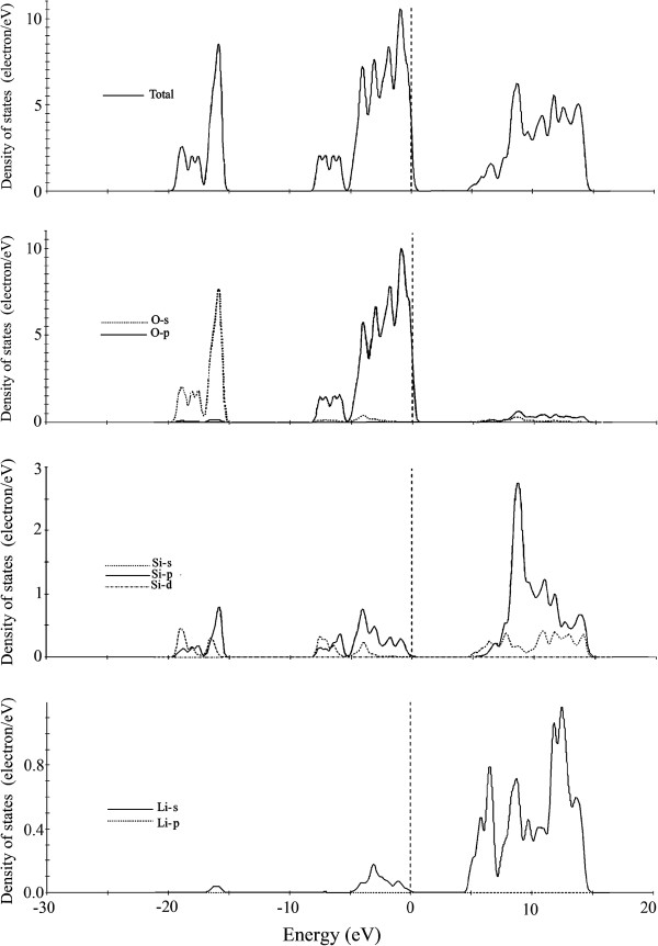
Figure 9

The most complex VBs are from -8.07 eV in Li 2 SiO 3 and -8.84 eV in Li 2 Si 2 O 5 to the Fermi level (0.0 eV). According to the partial density of states, it is confirmed that the valence bands at these energy intervals are essentially formed by O-2 p for both compounds, along with small admixture Li-2 s , while the contributions from Si-3 s , 3 p states in Li 2 Si 2 O 5 are significant and cannot be neglected. Such characteristic indicates that covalent bonds could be formed among O-2 p and Si-3 p , 3 s states in Li 2 Si 2 O 5 . However, in the case of Li 2 SiO 3 , these contributions are weaker. The valence bands at these energy ranges can be further divided into two parts. Such a splitting characteristic of valence bands reflects different bonding behaviors. The first parts located at -8.84 to -5.19 eV (for Li 2 SiO 3 ) and -8.07 to -4.62 eV (for Li 2 Si 2 O 5 ) are due to the bonding between Si-3 s , 3 p , Li-2 s orbits and O-2 p orbits, while the second part from -5.19 to -4.62 eV for Li 2 SiO 3 and Li 2 Si 2 O 5 , respectively, to the Fermi level (0.0 eV) indicates the small interaction between Si-3 p , Li-2 s orbits and O-2 p orbits. Analyzing the PDOS also suggests ionic interactions between Si-2 s , 2 p orbits and O-2 s , 2 p orbits.
The conduction bands between 4.23 and 14.61 eV for Li 2 SiO 3 come from Si-3 s , 3 p states, Li-2 s states, and O-3 s , 3 p states. In comparison, the bands between 4.23 and 10.00 eV for Li 2 Si 2 O 5 come primarily from Si-3 p states, with small contribution from Si-3 s states, Li-2 s states, and O-2 s , 2 p states. The hybridization between Si-3 s , 3 p orbits and O-2 s , 2 p orbits at upper valence bands is the important structural character of the two compounds.
Optical properties
The optical properties can be gained from the complex dielectric function [
50
,
51
]:
This is mainly connected with the electronic structures and characterizes the linear response of the material to an electromagnetic radiation, and therefore governs the propagation behavior of radiation in a medium. The imaginary part of the dielectric function
ε
2
(
ω
) represents the optical absorption in the crystal, which can be calculated from the electronic structure through the joint density of states and the momentum matrix elements between the occupied and the unoccupied wave functions within the selection rules and is given
where
e
is the electronic charge, and
The real part
ε
1
(
ω
) is evaluated from the imaginary part
ε
2
(
ω
) by the Kramers-Kronig transformation. The other optical constants such as the refractive index
n
(
ω
), extinction coefficient
k
(
ω
), optical reflectivity
R
(
ω
) absorption coefficient
α
(
ω
), energy loss spectrum
L
(
ω
), and the complex conductivity function
σ
(
ω
) can be computed from the complex dielectric function
ε
1
(
ω
), through the following relations [
49
,
50
]:
The dielectric functions of Li
2
SiO
3
and Li
2
Si
2
O
5
were calculated based on the electronic structure. The
ε
1
(
ω
) and
ε
2
(
ω
) as a function of the photon energy are shown in Figure
10
for Li
2
SiO
3
and Li
2
Si
2
O
5
.
Dielectric functions of Li
2
SiO
3
(top) Li
2
Si
2
O
5
(bottom).Figure 10

The imaginary part of ε ( ω ) in Li 2 SiO 3 has three intense bands located at 9.02, 11.11, and 14.35 eV. The first peak corresponds mainly to the transition from O-2 p states (VBs) to the empty Li-2 s and Si-3 s states (CBs) above the Fermi level. The second and third peaks are mainly due to the transitions from O-2 p states (VBs) to the Si-3 p and Li-2 s states (CBs) above the Fermi level. In contrast, Li 2 Si 2 O 5 has a prominent absorption peak, located at the photon energies of 9 eV and two weaker bands located at 11.74 and 15 eV. The main peak at the 9 eV is due to strong interband transitions between the O-2 p states (VBs) and Si-3 p empty states (CBs). It is noted that a peak in ε 2 ( ω ) does not correspond to a single interband transition since many direct or indirect transitions may be found in the band structure with an energy corresponding to the same peak [ 52 ]. The peak amplitudes of Li 2 SiO 3 are larger than those of the Li 2 Si 2 O 5 crystals, due to the fact that the band structures for the two compounds are not similar.
For the real part
ε
1
(
ω
) of the dielectric function
ε
(
ω
), the most important quantity is the 0 frequency limit
ε
1
(0), which is the electronic part of the static dielectric constant and depends strongly on the band gap. A smaller energy gap yields a larger
ε
1
(0) value. This could be explained on the basis of the Penn model [
52
]:
The energy gap (
E
g
) could be determined from this expression by using the values of
ε
1
(0) and the plasma energy h
ω
p
. The calculated and experimental
E
g
and also the calculated static dielectric constants
ε
1
(0) of Li
2
SiO
3
and Li
2
Si
2
O
5
are listed in Table
1
.
Theoretical and experimental energy gaps (
E
g
) and the calculated average static dielectric constant of Li
2
SiO
3
and Li
2
Si
2
O
5 Li2SiO3 Li2Si2O5 Calculated Experimental Calculated Experimental Pseudo-potentials Norm-conserving - Norm-conserving - 4.575 4.49 (a) 4.776 4.56 (a) 4.51 (b) 4.53 (b) 4.51 (c) 4.48 (c) 2.39 - 1.70 -Table 1
The calculated results on the absorption, reflectivity, and energy loss spectra by norm-conserving pseudo-potentials were shown in Figures
11
,
12
,
13
. According to the absorption spectra, the absorption edges are located at 9.11, 11.85, and 14.70 eV for lithium metasilicate and at 8.2, 11.60, and 15 eV for lithium disilicate. The absorption coefficients decrease rapidly in the low-energy region, which is the representative character of the semiconductors and insulators.
Calculated absorption spectra of Li
2
SiO
3
(top) and Li
2
Si
2
O
5
(bottom). Calculated reflectivity of Li
2
SiO
3
(top) and Li
2
Si
2
O
5
(bottom). Calculated energy loss function for Li
2
SiO
3
(top) and Li
2
Si
2
O
5
(bottom).Figure 11
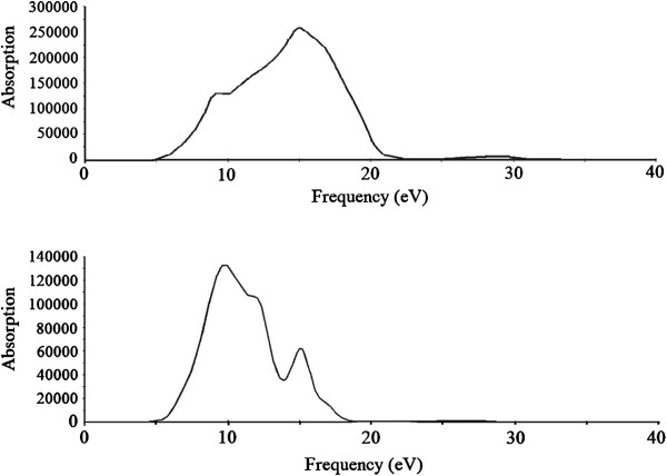
Figure 12

Figure 13

The calculated reflectivity for lithium metasilicate at 0 to 5 eV is lower than 10% and a maximum value of roughly 35.0% is calculated at about 17.53 eV. In comparison, the reflectivity for lithium disilicate at 0 to 5 eV is calculated to be lower than 2%. The calculated reflectivity spectrum of lithium disilicate shows a maximum value of about 15% at 9.9 eV. According to the absorption and reflectivity spectra, it is concluded that lithium metasilicate and lithium disilicate are transmitting for frequencies of <4.00 eV.
The energy loss spectrum describes the energy loss of a fast electron traversing in the material [ 53 ]. The main peak is generally defined as the bulk plasma frequency [ 54 ]. At energies smaller than 5.0 eV, no distinct peak is calculated due to the fact that ε 2 ( ω ) is still large at these energy values. The main peaks of energy loss spectra, as shown in Figure 13 , are calculated at about 12.82 and 15.55 eV for lithium disilicate and 19.5 eV for lithium metasilicate. Such calculations may stimulate the experimental investigations.