Centre for Research in Nanotechnology and Science (CRNTS), Indian Institute of Technology Bombay, Powai, Mumbai, 40076, IN
Abstract
It has been possible to incorporate cadmium ions in ZnS quantum dots (QDs). It is studied how the substitution of Cd
2+
ions by zinc ions affects the structural, morphological, and optical properties of ZnS QDs. Zn
1−
x
Cd
x
S QDs are prepared by a simple beaker chemistry approach and characterized by X-ray diffraction (XRD), high-resolution transmission electron microscopy, and UV-visible and photoluminescence (PL) spectroscopies. XRD studies confirmed that all the prepared samples are in zinc-blende phase. With the increase of cadmium content, the diffraction peaks shifted towards lower diffraction angles and the lattice constant increased linearly. Optical studies revealed that the strong absorption edge also shifted towards the higher wavelength region with the increase of Cd content. Hence, the optical bandgap of the QDs decreases with the increase of Cd content. Due to the quantum confinement of the carriers in the QDs, the bandgap energy is higher than that of the corresponding bulk material. The PL spectrum of the undoped ZnS QDs contains five peaks (centered at 365, 400, 420, 450, and 470 nm) which are attributed to the recombination of the defect states of ZnS.
Background
Nanocrystalline solid solutions are very attractive materials because of their potential to control the optical properties by varying the solution composition as well as the particle size. In the case of ZnS, the bandgap varies in the range of 3.7 to 5.5 eV depending upon the particle size in the nanoregime [
1
,
2
]. However, by incorporating Cd
2+
ions into ZnS nanocrystals, Zn
1−
x
Cd
x
S solid-solution semiconductors have been made and their energy bandgap was found to vary from 5.5 to 2.5 eV at room temperature [
2
–
4
]. As a consequence, the absorption edge shifts towards lower energy with the increase of Cd content. The quantization of bandgap in ZnS shows blue-green emission arising from defect states [
2
,
5
]. However, the emission spectra of cubic cadmium-doped ZnS (ZnS:Cd) quantum dots (QDs) were reported to cover the entire visible spectrum by varying the Cd
+2
/Zn
+2
ratios [
6
,
7
].
Herein, a simple beaker chemistry approach is demonstrated to synthesize ultra-fine Zn
1−
x
Cd
x
S QDs at room temperature. Transmission electron microscopy (TEM) results confirm that the incorporation of Cd ions (
x
from 0 to 0.5) in ZnS QDs leads to an increase in the particle size from 4 to 7 nm. A similar trend for the increases of particle size with Cd content is also observed from X-ray diffraction (XRD) and UV-visible measurements. Photoluminescence spectra show an increase of the strain on the QD surface with the increase of Cd content, and it leads to increases in the intensity of the 470-nm peak.
Methods
Zn
1−
x
Cd
x
S (0 ≤
x
≤ 0.5) QDs were prepared at room temperature without using any capping agent or surfactant via beaker chemistry. The preparation of Zn
1−
x
Cd
x
S nanocrystallite powders was carried out in two steps. In the first step, two different solutions, solution I and solution II, were prepared separately. Solution I was prepared by dissolving an appropriate amount of cadmium acetate dihydrate and zinc acetate dihydrate such that the total amount of these two salts was 10 mmol in 30 ml methanol. In solution II, a saturated solution of sodium sulfide monohydrate was prepared by dissolving Na
2
S in 20 ml methanol. In the second step, solution I was first vigorously stirred using a magnetic stirrer for 30 min, and then solution II was added to solution I dropwise and stopped when the pH of the solution becomes 8. The whole reaction was carried out at room temperature. The mixed thick solution was stirred for 1 h to complete the chemical reaction. The precipitate was separated by centrifugation at 8,000 rpm for 6 min and washed several times with methanol to remove sodium ions. Then the washed precipitate was dried to collect the finally prepared Zn
1−
x
Cd
x
S QDs. The Cd composition
x
was controlled as 0, 0.01, 0.04, 0.1, 0.2, 0.3, and 0.5. A brief pictorial detail of the synthesis procedure is given in Figure
1
.
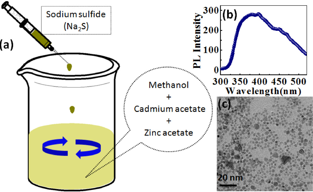
Figure 1
Schematic representation of Zn1−xCdxS QD synthesis, defect-related blue emission, and TEM micrograph of 4-nm ZnS QDs.
(
a
) Schematic representation of Zn
1−
x
Cd
x
S QD synthesis via simple beaker chemistry. (
b
) Defect-related blue emission obtained from 4-nm ZnS QDs. (
c
) TEM micrograph of 4-nm ZnS QDs produced from 5 mmol Zn precursor in 30 ml methanol.
The X-ray diffraction pattern confirmed the formation of Zn
1−
x
Cd
x
S phase. The X-ray diffraction pattern was recorded using an X-ray diffractometer (PANalytical, Almelo, The Netherlands) using Cu Kα radiation of wavelength
λ
= 0.15406 nm. The transmission electron microscope (JEOL JEM 2100F, Akishima-shi, Japan) study confirmed the formation of Zn
1−
x
Cd
x
S QDs. The optical transmission/absorption spectra of Zn
1−
x
Cd
x
S QDs were recorded using a UV–Vis spectrophotometer (U-3010, Hitachi, Chiyoda-ku, Japan). For optical measurement, the sample powders were dispersed in methanol. The photoluminescence (PL) spectrum of Zn
1−
x
Cd
x
S QDs dispersed in methanol was measured using a spectrofluorimeter (F-2500 FL Spectrophotometer, Hitachi).
Results and discussion
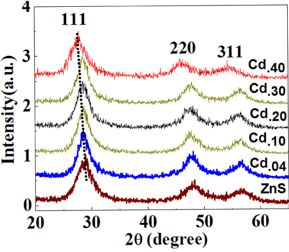
Figure
2
shows the XRD patterns of the Zn
1−
x
Cd
x
S QDs for different values of
x
(mole percentage of cadmium), which indicates that all samples are of zinc-blende (cubic) structure (JCPDS card no. 5–566) [
8
]. The characteristic XRD patterns of Zn
1−
x
Cd
x
S QDs exhibit three prominent peaks which correspond to (111), (220), and (311) planes of the cubic phase of ZnS with the lattice constant
a
= 5.4 Å (JCPDS card no. 80-0020) [
9
]. The diffraction peak positions also gradually shifted towards lower diffraction angles as the Cd concentration increased from 0 to 0.5, which indicates that the crystals obtained are not a mixture of pure ZnS and CdS rather a Zn
1−
x
Cd
x
S solid solution [
8
,
10
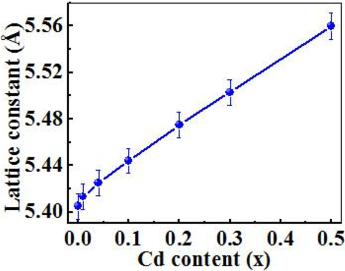
]. The variation of lattice parameter
a
estimated from XRD data with
x
is shown in Figure
3
, which shows a linear increase of the lattice constant from 5.405 to 5.560 Å with the increase of Cd content
x
from 0 to 0.5. A similar trend has also been reported earlier [
10
,
11
]. This linear increase in lattice parameter
a
with the increase of Cd content confirms the formation of a homogenous solid solution of Zn
1−
x
Cd
x
S nanostructure. The small difference in the bond length of ZnS and CdS and the very close electronegativity value of Cd and Zn allow the formation of solid-solution materials.
Figure 2
XRD patterns of the Zn1−xCdxS QDs produced with different mole fractions (x) of Cd.
Figure 3
Variation of the lattice parameter with Cd content in ZnS QDs.
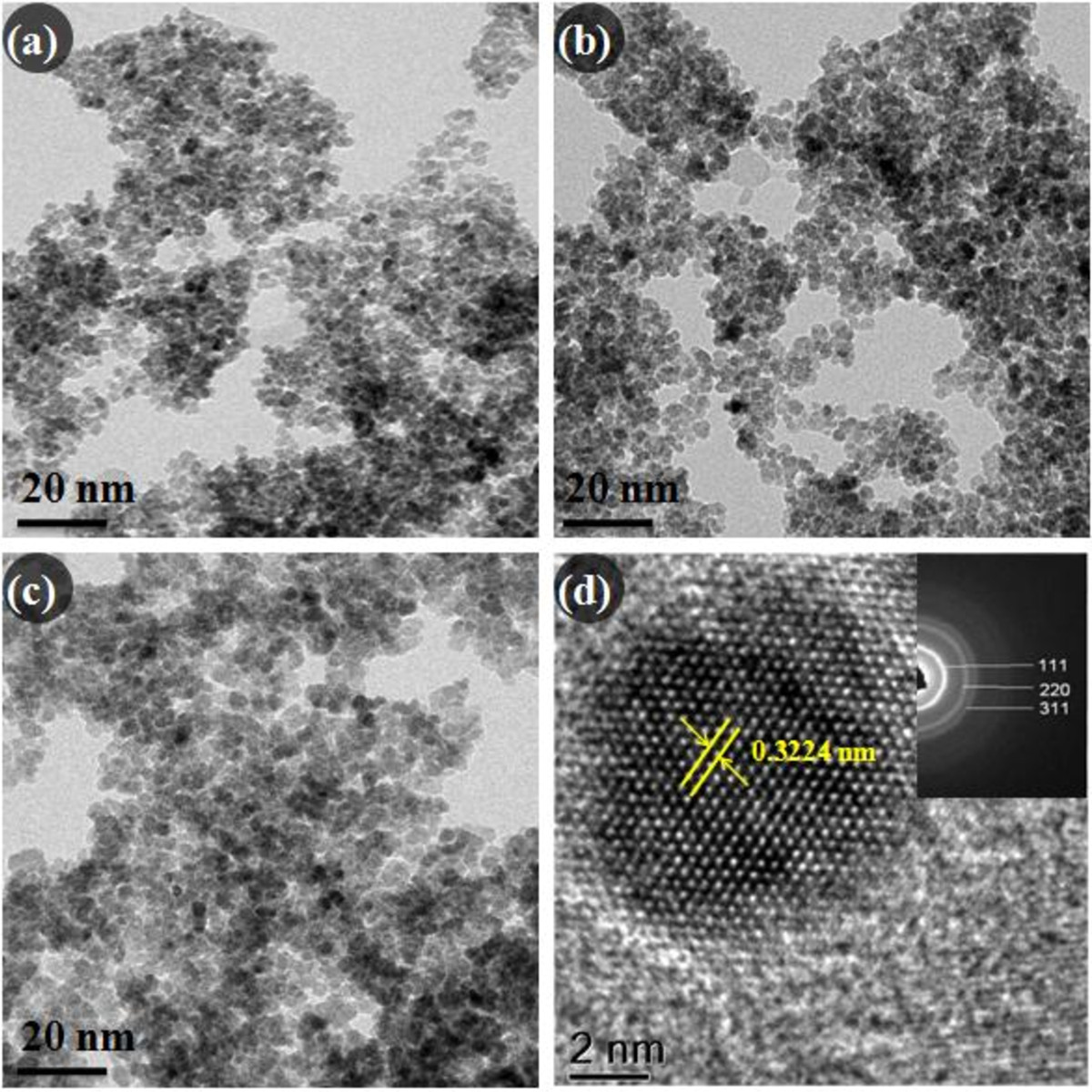
Figure
4
a,b,c shows the TEM images of Zn
1−
x
Cd
x
S QDs having Cd concentrations of 0.04, 0.1, and 0.5, respectively. The average particle sizes estimated are 4.5 ± 0.5 nm (
σ
= ±10%) for the
x
= 0.01 sample, 5 ± 0.5 nm (
σ
= ±10%) for the
x
= 0.1 sample, and 7 ± 1 nm (
σ
= ±15%) for the
x
= 0.5 sample, and this is consistent with the particle sizes estimated from XRD spectra (by using the Scherrer formula; see Table
1
). Figure
4
d shows the high-resolution transmission electron microscopy (HRTEM) image of QDs produced with Cd concentration
x
= 0.5 which confirms the crystallinity of the as-synthesized QDs. The inset of Figure
4
d represents the selected-area electron diffraction (SAED) pattern. As expected, the SAED pattern shows a set of rings instead of spots due to the random orientation of the crystallites, corresponding to reflections from three crystal planes: (111), (220), and (311). This confirms the formation of a cubic phase of ZnS. The interplanar spacings (
dhkl
) calculated from XRD and SAED are summarized in Table
2
for Zn
1−
x
Cd
x
S (with
x
= 0.04, 0.1, 0.5). Figure
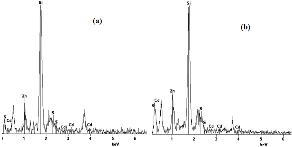
5
a,b shows the energy-dispersive X-ray (EDAX) spectra of the Zn
1−
x
Cd
x
S QDs with Cd atomic fraction
x
= 0.04 and 0.1, respectively, which confirms the stoichiometric composition of the prepared samples.
Figure 4
Representative TEM images of Zn1−xCdxS QDs and HRTEM image of a single QD.
TEM images of Zn
1−
x
Cd
x
S QDs with Cd content of (
a
)
x
= 0.04, (
b
)
x
= 0.1, and (
c
)
x
= 0.5. (
d
) HRTEM image of a single QD produced with Cd content
x
= 0.5, and the inset shows the SAED pattern.
Table 1
Comparison of bandgap energy and size of Zn1−xCdxS QDs produced with different Cd concentrations
Cd concentration (%)
Optical bandgap energy of nanocrystalEg(eV)
Particle size from XRD (nm)
Particle size estimated from UV-vis data (nm)
1
4.1
4.8
4.6
4
4.0
5.1
5.0
10
3.9
5.4
5.1
20
3.8
5.9
5.5
30
3.7
6.4
5.9
50
3.4
6.8
6.3
Table 2
Comparison of interplanar spacing (d111) obtained from XRD and SAED for Zn1−xCdxS QDs withx= 0.04, 0.1, and 0.5
Sample name
d111from XRD (nm)
d111from SAED (nm)
Particle size from TEM (nm)
Zn.96Cd.04S
0.312
0.312
5 ± 0.5
Zn.90Cd.10S
0.313
0.314
6 ± 0.5
Zn.50Cd.50S
0.3254
0.323
7 ± 1
Figure 5
Determination of stoichiometric ratio for Zn1−xCdxS QDs.
EDAX spectra of Zn
1−
x
Cd
x
S QDs produced with Cd content of (
a
)
x
= 0.04 and (
b
)
x
= 0.1.
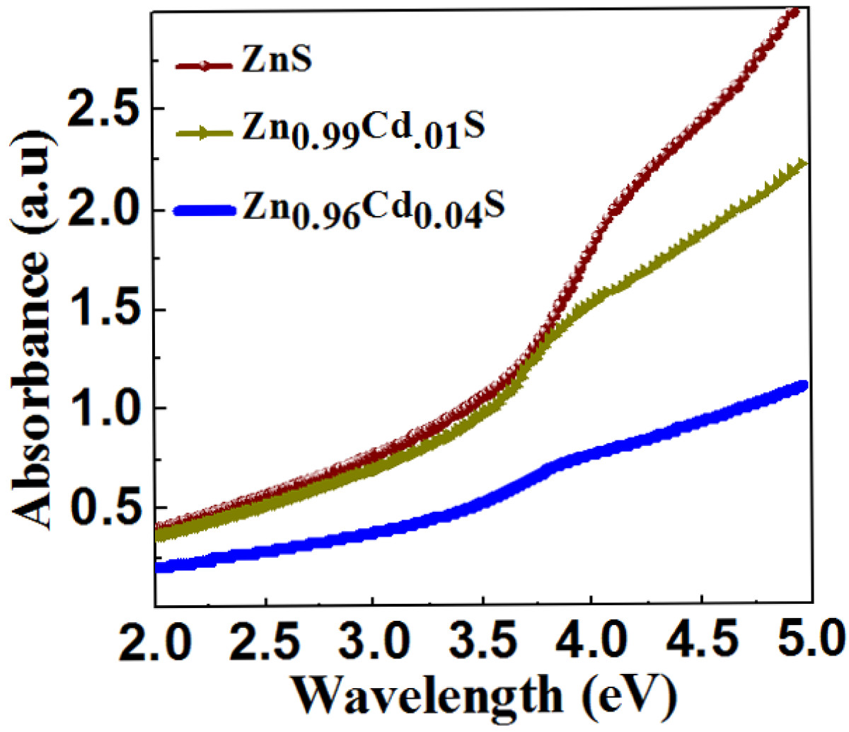
Figure
6
shows the UV-visible absorption spectra of the Zn
1−
x
Cd
x
S QDs. In pristine ZnS QDs, the excitonic peak appears at a wavelength around 312 nm. This peak position reflects the excitonic binding energy of QDs. Moreover, with increases of Cd content in ZnS, the excitonic peak which is a characteristic of QDs gradually shifts towards a higher wavelength. The red shift is attributed to quantum confinement effect as well as the increase of Cd concentration (as the particle size increases with respect to the increases of Cd content) [
12
].
Figure 6
UV-visible absorption spectra of the as prepared Zn1−xCdxS QDs dispersed in methanol.
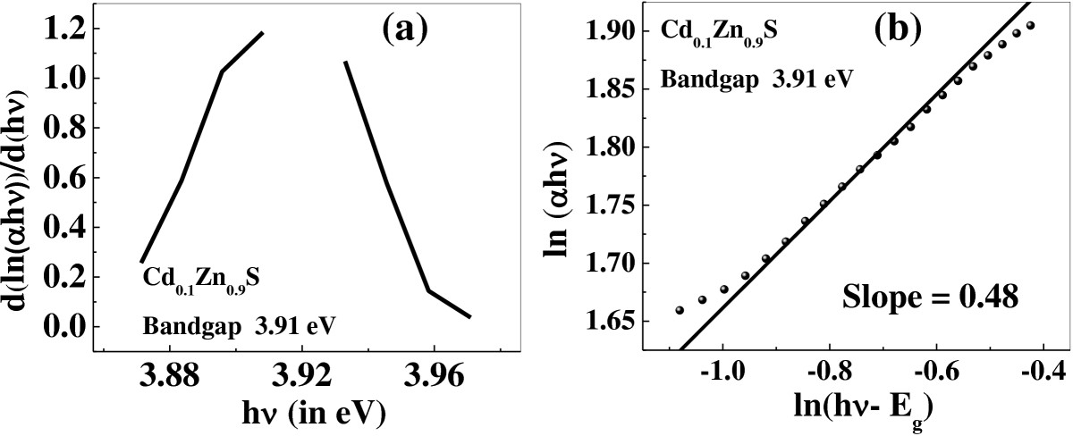
The fundamental absorption, which corresponds to the transition from the valence band to the conduction band, can be used to determine the optical bandgap of the material. From the transmission data, the absorption coefficient (
α
) at different wavelengths
λ
is calculated using Beer-Lambert’s relation (reflection/scattering is negligible due to the small size of the particle), given by
α=1dln1T
The relation between
α
and the incident photon energy (
hν
) can be written as [
12
]
α=Ahνhν−Egm
where
A
is a constant,
Eg
is the bandgap of the material, and the exponent
m
depends on the type of transition. The exponent
m
has the values 1/2, 2, 3/2, and 3 corresponding to the allowed direct, allowed indirect, forbidden direct, and forbidden indirect transitions, respectively. The bandgap can be estimated from the plot of (
αhν
)
1
/m
versus
hν
, where
m
indicates the nature of optical transition in the material. For bulk semiconductors with direct transition,
m
= 0
.
5. In a nanocrystalline material, the nature of optical transition can be different from that in the bulk as mentioned earlier. Therefore, to avoid any preassumption, the values of
m
for Zn
0.9
Cd
0.1
S QDs were determined as discussed below. Now Equation
2
can be written as follows:
dlnαhνdhν=mhν−Eg
So, there should be a discontinuity in the
d
(ln(
αhν
))/
d
(
hν
) versus
hν
plot at the bandgap energy. A representative plot of
d
(ln(
αhν
))/
d
(
hν
) versus
hν
is presented in Figure
7
a, showing a divergence at
hν
=
Eg
. Using the value of
Eg
thus obtained, we can determine the value of
m
and hence the nature of transition. Again, from Equation
2
, we can get
lnαhν=lnA+mlnhν−Eg
Figure 7
Determination of the bandgap and the nature of transition for Cd0.1Zn0.9S QDs.
(
a
)
d
(ln(
αhν
))/
d
(
hν
) versus
hν
curve showing a divergence at
Eg
= 3.91 eV and (
b
) ln(
αhν
) versus ln(
hν
−
Eg
) curve.
The value of
m
was determined from the slope of the plot of ln(
αhν
) versus ln(
hν − Eg
). The slope in Figure
7
b gives the value of
m
. Using this method, we calculated the value of
m
for Zn
0.9
Cd
0.1
S QDs (0.48) which is comparable to that for direct allowed transition in the bulk material (
m
= 0
.
5). For all the prepared samples, the values of
m
are found to be close to the value for the bulk. Now the value of the bandgap can be estimated from the plot of (
αhν
)
2
versus
hν
, as shown in Figure
8
. By extrapolating the straight portion of the graph on the
hν
axis at
α
= 0, the optical bandgaps are calculated, and the values are summarized in Table
1
. The obtained bandgap energy is higher than that of the bulk material. Moreover, the bandgap energy decreases with the increase of Cd content in the ZnS QDs [
10
,
12
]. This supports the TEM results that the increases of Cd content result in the increases of the QD size. The optical bandgap of QDs is a combination of the quantum confinement effect arising due to the confinement of the charge carriers and the differences between excitonic energy levels. The quantum confinement resulted to a blue shift of the absorption edge; on the other hand, the excitonic energy caused the red shift of the absorption edge. The observed high values of the optical bandgap energy and its blueshifts with Cd content confirm the formation of Zn
1−
x
Cd
x
S QDs. The bulk bandgap energy for different Cd compositions can be obtained from the empirical relation [
13
,
14
] given by
Egx=EgZnS+EgCdS−EgZnS−0.61x+0.61x2
Figure 8
Calculation of the optical bandgap from the UV-visible absorption spectra.
The incorporation of Cd
2+
into the ZnS lattice site increases the excitonic energy of the Zn
1−
x
Cd
x
S QDs, and as a result, a red shift of the absorption edge is observed. According to the theory for the quantum size effect, the lowest exciton energy in a spherical nanoparticle with a radius
R
is approximately given by [
14
]
E=Eg+h28μR2−1.8e2ϵR
where
Eg
,
μ
, and
ϵ
are the bandgap, reduced mass, and dielectric constant, respectively. Since the values of
Eg
,
μ,
and
ϵ
depend on
x
in alloy semiconductors, Equation
6
can be modified as follows:
E=Egx+h28μxR2−1.8e2ϵxR
The reduced mass can be obtained by estimating the effective mass of the electron and hole. The band-edge effective mass
me*
of the carrier can be expressed as [
12
]
mme*=1m*=1+P22mEg
So the bandgap
Eg
can be expressed as
Eg=P22mm*1−m*=P22mfm*
where
m*=me*m
, with
m
being the mass of the free electron, and
P
is the momentum matrix element which can be expressed as
P=ℏG
, where
G
is the smallest reciprocal lattice vector. Therefore,
P
becomes equal to
ha
, where
a
is the lattice constant, and
fm*=m*1−m*
Using Equation
9
in Equation
5
, we obtain
fm*,x=fm*1+fm*2−fm*2−b+bx2,
where
b=.61P22m
and
m1*
and
m2*
correspond to the effective masses of the carriers of constituent semiconductors. For the Zn
1−
x
Cd
x
S crystal, the
b
value was found to be 0.06:
fm*,x=fm*1+fm*2−fm*2−0.61x+0.61x2.
Therefore, by estimating the effective mass of the different values of
x
, we can calculate the average particle size for the different compositions of semiconductor (using Equation
6
). The calculated particle sizes for Zn
1−
x
Cd
x
S QDs are summarized in Table
1
. The value of the dielectric constant for ZnS is 5.4, and for CdS, it is 5.3. Since there is no appreciable difference between the dielectric constant values of ZnS and CdS, for the calculation of particle size, we have taken
ϵ
(
x
) = 5.4 for all samples. The calculated values of the size of the QDs are well agreed with the value obtained from the X-ray diffraction and TEM analysis.
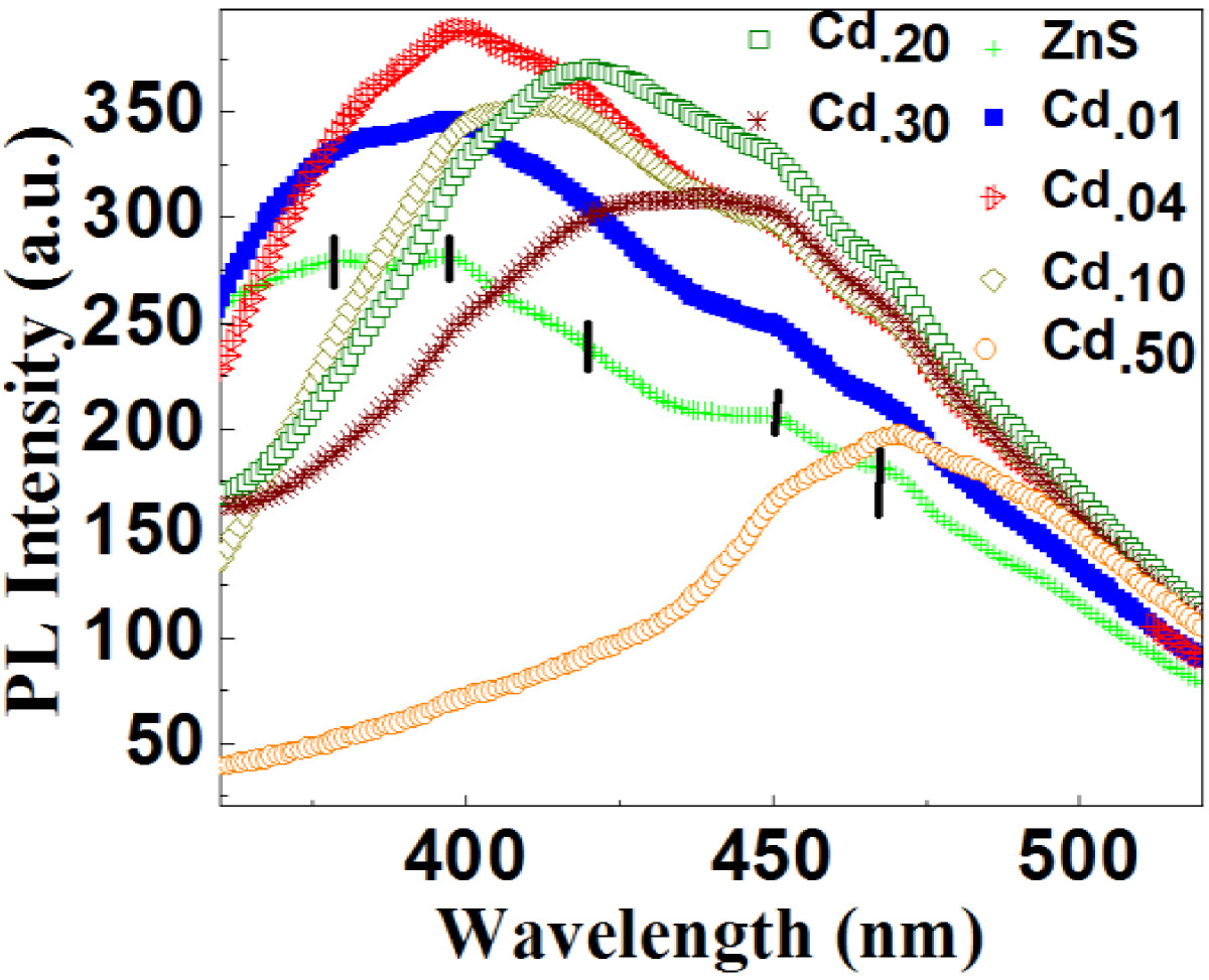
The room-temperature PL spectra of the Zn
1−
x
Cd
x
S QDs are shown in Figure
9
. The PL emission spectrum of the neat ZnS QD shows a highly broadened defect emission band with multiple peaks at 378, 400, 420, 450, and 470 nm. The high-energy side bands (400 and 420 nm) are attributed to the presence of a large concentration of sulfur vacancy centers in the QDs [
15
,
16
], whereas the first peak (378 nm) of the emission is attributed to the blue emission from interstitial sites [
17
]. The fourth and fifth peaks at 450 and 470 nm are related to the blue emission from zinc vacancy and surface defects, respectively. From Figure
9
, it can be seen that the peak intensities at 378, 400, and 420 nm for the pure ZnS sample are much smaller than those for the doped samples. It can be explained by the effect of doping. As analyzed above, these peaks are related to native defects. When Cd
2+
ions are incorporated into ZnS QDs, more defect states are introduced. Therefore, it is reasonable that these defect-related peak intensities are enhanced for the Zn
1−
x
Cd
x
S samples compared with the pure ZnS sample. Above 30% doping, the PL peak at 470 nm, due to the lattice defect, dominates all other peaks, although the overall PL intensity decreased at the Cd concentration of 30%. This is due to increase of the surface defect state in Zn
1−
x
Cd
x
S crystals. As the concentration of Cd
2+
increased, it is observed that there is a slight shift in peak position. This shift is due to the increase of particle size and also supports the formation of a Zn
1−
x
Cd
x
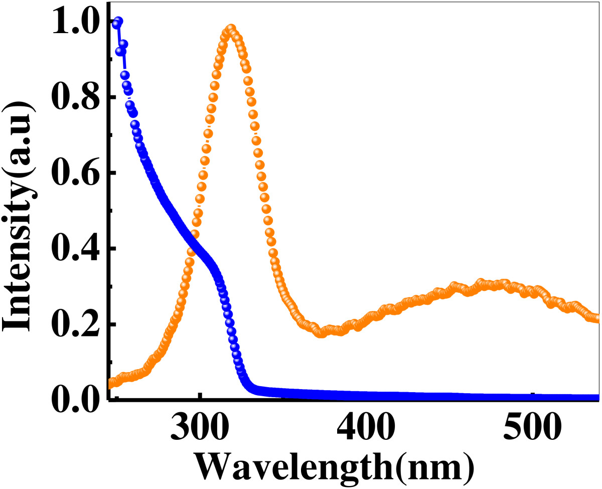
S nanocrystalline solid solution. All these defect-related emissions can be controlled by functionalizing the prepared QDs with long-chain amine. As-prepared Zn
0.9
Cd
0.1
S QDs (100 mg) were mixed with a mixture of 8 ml 1,2-dichlorobenzene and 5 ml oleylamine at room temperature. Under N
2
ambience, the mixture solution was continuously stirred at 150°C for 2 h. After the reaction, the sample was collected by centrifugation at 7,000 rpm for 4 min and washed several times with the acetone and hexane mixture. Figure
10
shows the UV-visible and PL spectra of the amine-functionalized Zn
0.9
Cd
0.1
S QDs. The amine ligands (σ-donor) take the position of the vacancies and control the symmetry of the surface closer to that of the core. This phenomenon assists in the compression of the surface defects on the nanoparticle surface by repairing the broken and dangling bonds [
18
]. This defect-controlled Zn
1−
x
Cd
x
S nanocrystalline solid solution can have a wide range of applications including UV light-emitting diodes, efficient phosphors in flat-panel displays, photovoltaic devices, etc.
Figure 9
PL emission spectra of Zn1−xCdxS QDs dispersed in methanol.
Figure 10
UV-visible (blue line) and PL (orange line) spectra for amine-functionalized Zn0.9Cd0.1S QDs.
Conclusion
Zn
1−
x
Cd
x
S QDs with different compositions (0 <
x
< 0.5) are successfully synthesized by simple beaker chemistry without using any capping agent or surfactant. X-ray diffraction study confirmed the proper cubic phase formation. Due to the increase of Cd content, all the XRD peaks shifted towards lower diffraction angles. The lattice constant also gradually increased with the Cd content. The XRD results and TEM images showed that uniform spherical particles were formed and particle sizes varied from 4 to 7 nm as the Cd content was increased from 0 to 0.5. Optical study revealed that the strong absorption edge shifted towards the higher wavelength region; hence, the optical bandgap of the materials decreased with the increase of Cd content. Due to the quantum confinement effect of QDs, the optical bandgap energy is higher than the corresponding value of the bulk material. The PL spectra of the samples are broad and asymmetric and contain five blue emission peaks related to native defects of ZnS.
Acknowledgements
Heartfelt thanks to Dr. Soumen Basu, Physics Dept., NIT Durgapur, for guiding the author in various ways during his research work. The author is grateful to the National Institute of Technology, Durgapur, for supporting this research work.
Competing interests
The author declares that he has no competing interests.
References
Tomihira et al. (2005) Optical properties of ZnS–CdS alloy quantum dots prepared by a colloidal method10.1016/j.jlumin.2004.09.011
Sarkar et al. (2008) Yellow-orange light emission from Mn2+-doped ZnS nanoparticles10.1016/j.physe.2008.04.013
Wang et al. (2008) Composition-controllable synthesis and optical properties of non-integral stoichiometry compound ZnxCd1dxS nanorods10.1016/j.jallcom.2006.12.046
Peny and Ping (2001) Formation of high-quality CdTe, CdSe, and CdS nanocrystals using CdO as precursor10.1021/ja003633m
Arora and Manoharan (2008) Structural and photo luminescent properties of uncapped nanocrystalline Cd1-xZnxS solid solutions10.1016/j.optmat.2008.02.011
Leverenz (1950) Wiley
Zu et al. (2009) Synthesis of nano-CdxZn1-xS by precipitate-hydrothermal method and its photocatalytic activities10.1016/j.jallcom.2008.09.115
Tiwary et al. (2009) Synthesis of wurtzite-phase ZnS nanocrystal and its optical properties10.1016/j.jlumin.2009.07.004
Jana et al. (2007) Synthesis, structural and optical characterization of nanocrystalline ternary Cd1-xZnxS thin films by chemical process10.1016/j.physe.2007.01.009
Ray et al. (1998) Deposition and characterization of ZnxCd1-xS thin films prepared by the dip technique10.1016/S0040-6090(97)00932-2
Manzoor et al. (2005) Enhanced electroluminescence properties of doped ZnS nanorods formed by the self-assembly of colloidal nanocrystals10.1016/j.ssc.2005.04.001
Rao et al. (2007) Wiley
Arora and Manoharan (2007) Large shift in the photoluminescent properties of Mn2+-doped nanosized CdS–ZnS solid solutions10.1016/j.ssc.2007.08.038
Mohapatra et al. (2013) Surface controlled synthesis of MFe2O4 (M = Mn, Fe, Co, Ni and Zn) nanoparticles and their magnetic characteristics (pp. 524-532) 10.1039/C2CE25957E