CNR-IPCF UoS di Cosenza, Licryl Laboratory, and Centro di Eccellenza CEMIF.CAL, Università della Calabria, Rende (Cosenza), 87036, IT
Thin film Laboratory, Department of Physics, Sri Venkateswara University, Tirupati, 517 502, IN
Department of Energy, CIEMAT, Madrid, 28040, ES
Abstract
Vanadium pentoxide (V
2
O
5
) thin films were grown on indium tin oxide-coated flexible Kapton substrates by home-built activated reactive evaporation technique. Film depositions were carried out at optimised oxygen partial pressure of 1 × 10
−3
Torr and plasma power of 8 W, and we investigated their microstructural and opto-electrochromic properties as a function of substrate temperature. The V
2
O
5
films grown at
Ts
= 473 K exhibited a nano-crystalline nature as evidenced from X-ray diffraction, atomic force microscopy and Raman studies. The nano-crystalline films composed of vertical elliptical-shaped grainy morphology demonstrated a high optical transmittance of 75% with an estimated optical bandgap of 2.38 eV. The dry lithiated nano-crystalline V
2
O
5
films demonstrated an optical modulation of 36.1% with a coloration efficiency value of 26.2 cm
2
/C at a wavelength of 550 nm. As-deposited nano-crystalline V
2
O
5
thin films demonstrated a constant discharge capacity of about 60 μAh cm
−2
μm
−1
for a few cycles at room temperature in the potential window of 4.0 to 2.5 V.
Background
Around the globe, utilisation of ‘electrical energy’ has been increasing substantially and has become an inevitable source to fulfil the metropolitan human life needs, ever expanding industrialization and corporate companies' requirements[
1
,
2
]. It is noteworthy to mention that the major consumers of energy in an advanced society are the air-conditioning systems and utilisation of light energy even during daytime to maintain room atmospheric conditions in a comfortable state. In this regard, ‛renewable energy’ researcher's community has been striving for the best alternatives to reduce the consumption of ‘electrical energy’ and triggered their research towards electrochromic window technology. A unique property of thin-film system ‘to change colour due to an applied external impulse and change back to their original state by removing of external impulse’ is coined as chromism[
3
]. At present, the significance has been boosted with the realisation that the phenomena of chromism are of much interest in the fenestration technology as a means to achieve energy-saving benefits by controlling the performance by responding to the variation of brightness of the environment[
4
,
5
]. Transition metal oxides (TMOs) in thin-film configuration with diverse structures and chromogenic properties have been the foci of the research community in the outlook of their potential applications in the
current science and technology
[
6
]. Among the other chromogenic materials, vanadium pentoxide (V
2
O
5
) in thin-film configuration is one of the TMOs, which has been receiving much attention owing to its quite motivating structural, chemical and chromogenic properties and exceptional industrial applications such as electrochromic devices and optical memory devices[
7
–
9
]. Most of the researchers have prepared thin films of V
2
O
5
on various solid substrates by different thin-film deposition techniques and investigated their microstructural, optical, electrochromic and electrochemical properties in detail[
10
–
12
].
In the
current science and technology
, the designing and fabrication of thin-film coatings on flexible substrates have grown worldwide into a major challenging and novel research area for cutting-edge future-based technologies. These flexible substrates are unique than solid glass substrates due to the following reasons: they are flexible, so they can bend and stick to any curved shape object without altering their basic properties, weigh less, are easy to carry and dimensionally stable, resistant towards moisture and oxygen, and thermally stable, tough and chemically resistant[
13
]. It is well acknowledged that plasma thin-film deposition methods have been recognised as ‘promising and pioneered’ to grow nearly stoichiometric thin films at low substrate temperatures. Various physical and chemical vapour thin-film deposition techniques have been employed to grow thin films of V
2
O
5
, in which activated reactive evaporation (ARE) is one of the plasma-assisted physical vapour thin-film deposition techniques to grow nearly stoichiometric thin films with better uniformity at relatively lower substrate temperatures with higher deposition rates[
14
,
15
]. In this deposition technique, the reaction occurs predominantly in plasma; as a result, chemical composition of the films can be controlled by changing the ratio of reacting species. Few researchers have reported about the growth of metal oxide thin films on flexible substrates for electrochromic window applications[
16
]. However, the ‘prominence and necessity of future fenestration technological needs’ divulge the impetus scope to carry out the research towards flexible electrochromic devices with enriched electrochromic properties. Hence, in the present investigation, we deposited V
2
O
5
thin films on indium tin oxide (ITO)-coated flexible Kapton substrates (the glass transition temperature of the substrate is 673 K) by home-built activated reactive evaporation technique, studied their microstructural properties and reported a comparative study on optical and electrochromic properties of amorphous and nano-crystalline V
2
O
5
thin films. In parallel, we made an attempt to study electrochemical properties for as-deposited nano-crystalline V
2
O
5
films.
Methods
In the present investigation, nano-sized V
2
O
5
powder was synthesised via co-precipitation method[
17
]. The precursor was prepared using 5.8 g of ammonium metavenadate (NH
4
VO
3
, 99.99% purity, Aldrich Company Ltd., Dorset, England, UK) powder, which is dissolved in highly purified distilled water. The white-coloured precursor was acidified using 0.1 M HCl, and in parallel, the resultant compound was stirred continuously at a stirring rate of 300 rpm. The obtained intermediate compound was filtered and cleaned by conventional processes, and the end product was sintered in the presence of ambient atmospheric pressure conditions at 773 K to get dark orange-coloured and fine V
2
O
5
powder. The resultant sintered powder was used as a starting material to grow the thin films for further studies.
The home-built activated reactive evaporation technique was adopted to grow V
2
O
5
thin films with a thickness of 350 nm on ITO-coated flexible Kapton substrates[
18
]. The film depositions were carried out at optimised oxygen partial pressure of 1 × 10
−3
Torr, plasma power of 8 W and by varying the substrate temperature (
Ts
) in the range of 303 to 523 K. The base pressure in the deposition chamber was maintained as 1 × 10
−6
Torr, and thicknesses of the deposited films were controlled through a quartz crystal thickness monitor and found to be 350 nm. The microstructural characterizations were carried out using a computerised X-ray diffractometer (XRD) (model 3003 TT, Siefert Companies, Massillon, OH, USA) using CuKα1 radiation (λ = 0.15406 nm), scanning electron microscope (SEM) (EVO MA 15, Carl Zeiss Inc., Oberkochen, Germany) and atomic force microscope (AFM) (Dimension 3100 series, Digital Instruments, Tonawanda, NY, USA), and Raman spectroscopy measurements were performed at room temperature with Jobin Yvon U1000 double monochromator (HORIBA Ltd., Kyoto, Japan) using a 514.5-nm line of Argon (Spectra-Physics, Santa Clara, CA, USA) laser at a power density of 0.4 W/cm
2
. The optical transmittance measurements were carried out using Hitachi U-3400 UV–vis-NIR double spectrometer (Hitachi Ltd., Chiyoda-ku, Japan) in the wavelength range of 300 to 1,500 nm. The electronic conductivity measurements were carried out using a standard four-probe configuration set-up with direct current. The electrochromic coloration studies for V
2
O
5
thin films were performed by employing dry lithiation method. In this method, lithium niobate (LiNbO
3
) powder was heat-treated at 1,113 K under high vacuum to give off lithium atoms for insertion in the exposed V
2
O
5
films[
19
]. The electrochemical characterizations of grown V
2
O
5
films were conducted in an Ar-filled glove box using an electrochemical workstation (608 C series, CH Instruments, Inc., Austin, TX, USA). The cut-off potentials of the electrodes were set in the range of 4.0 to 2.5 V because the narrow-range and high voltage is reliable for a cathode. The discharging profiles of the deposited films were recorded by exposing the effective area of 1 cm
2
in contact with a liquid electrolyte (1 M LiClO
4
in propylene carbonate) at a constant current density of 20 μA/cm
2
and lithium foil used as an anode.
Results and discussion
X-ray diffraction studies
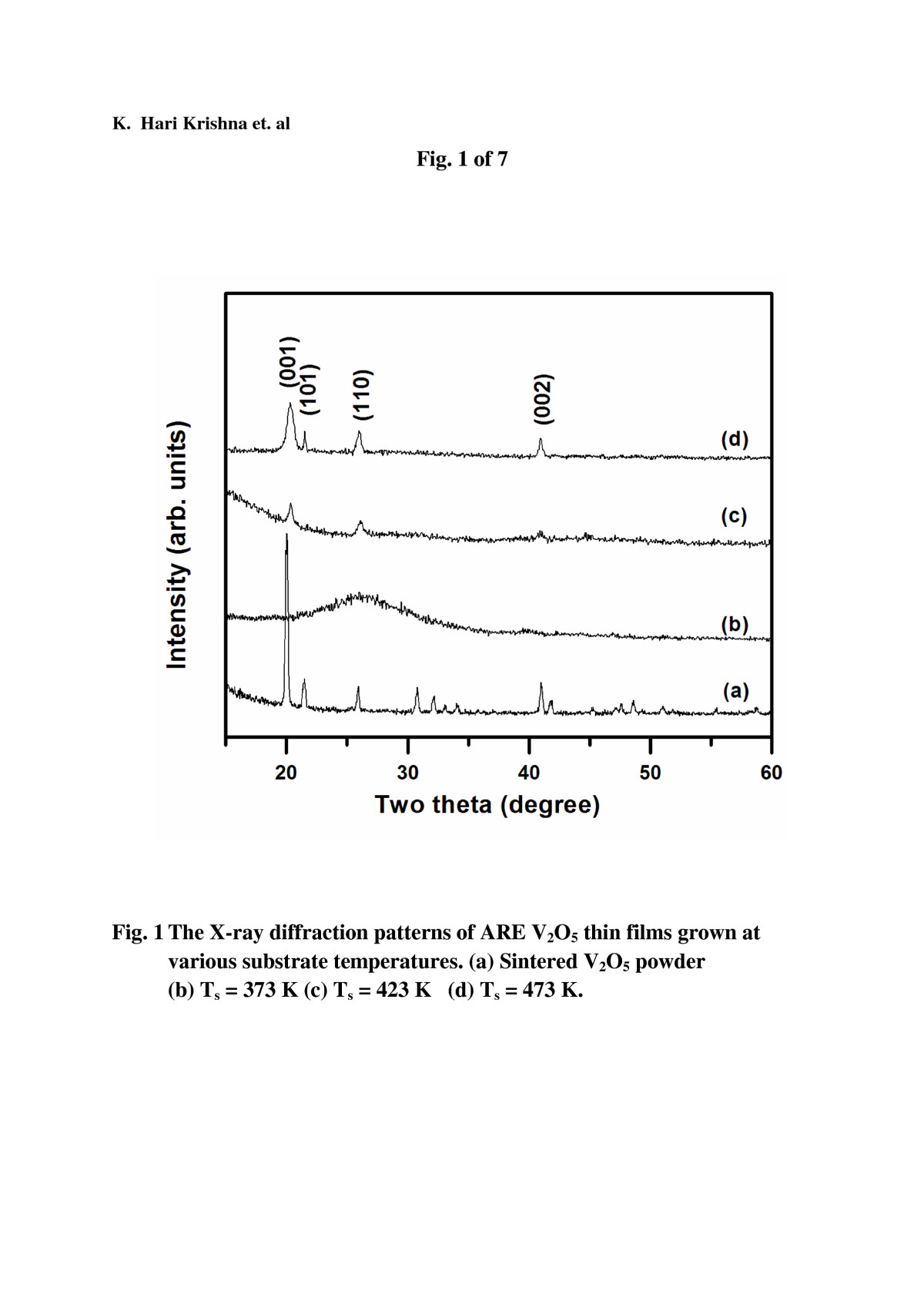
Figure
1
(curve a) displays the characteristic and relatively broad Bragg reflections present in the X-ray diffractogram of sintered V
2
O
5
powder, which reveals the presence of nano-crystalline nature of the powder. The evaluated lattice parameters were
a
= 1.152 nm,
b
= 0.356 nm and
c
= 0.443 nm, which are congruent with ‘JCPDS file 890612’[
20
]. The sintered V
2
O
5
powder was noticed to be composed of nearly rectangular flake-shaped nano-sized particles with the size of 30 nm as evidenced from an SEM picture (not shown). The estimated room temperature conductivity of as-sintered V
2
O
5
powder was in the order of 3.45 × 10
−4
Ω
−1
cm
−1
, which is nearly equal to the conductivity value of single-crystal V
2
O
5
(3.52 × 10
−4
Ω
−1
cm
−1
).
Figure 1
The X-ray diffraction patterns of ARE V2O5thin films grown at various substrate temperatures.
(curve a) Sintered V
2
O
5
powder, (curve b)
Ts
= 373 K, (curve c)
Ts
= 423 K and (curve d)
Ts
= 473 K.
The structural properties of grown V
2
O
5
thin films on flexible substrates were investigated by XRD technique. The as-deposited films grown at lower substrate temperatures (<423 K) demonstrated diffused and non-characteristic diffraction patterns (Figure
1
curve b), which indicate the amorphous nature of the films. The onset of crystallinity in the films was observed at a substrate temperature of 423 K, and respective X-ray diffractogram of the films displayed less intense diffraction peaks (001), (110) and (002), as represented in Figure
1
(curve c). The increase in crystallinity in the films was observed as a function substrate temperature, and for the films deposited at
Ts
= 473 K, the respective X-ray diffractogram exhibited relative broad and high intense characteristic diffraction peak at 2
θ
= 20.3°, which attributed to Bragg reflection from (001) lattice planes of orthorhombic V
2
O
5
. In addition to (001) Bragg reflection, the subsequent presence of characteristic orientations such as (101), (110) and (002) reveals the existence of in-plane organisation of V-O-V chains[
21
]. The relative predominance of (001) Bragg reflection reflects the growth of the films along the
c
-axis perpendicular to the surface of substrate in texture of the grown films. The evaluated lattice parameters for the film grown at
Ts
= 473 K are found to be
a
= 1.153 nm,
b
= 0.355 nm and
c
= 0.435 nm, which are congruent with powder data and previous reported values in the literature[
22
]. Scherer's formula is employed to estimate the size of crystallites, and it was found to be 90 nm for the films deposited at 473 K.
Raman studies
The Raman spectroscopic measurements were performed in the wavelength range of 200 to 1,200 cm
−1
for the V
2
O
5
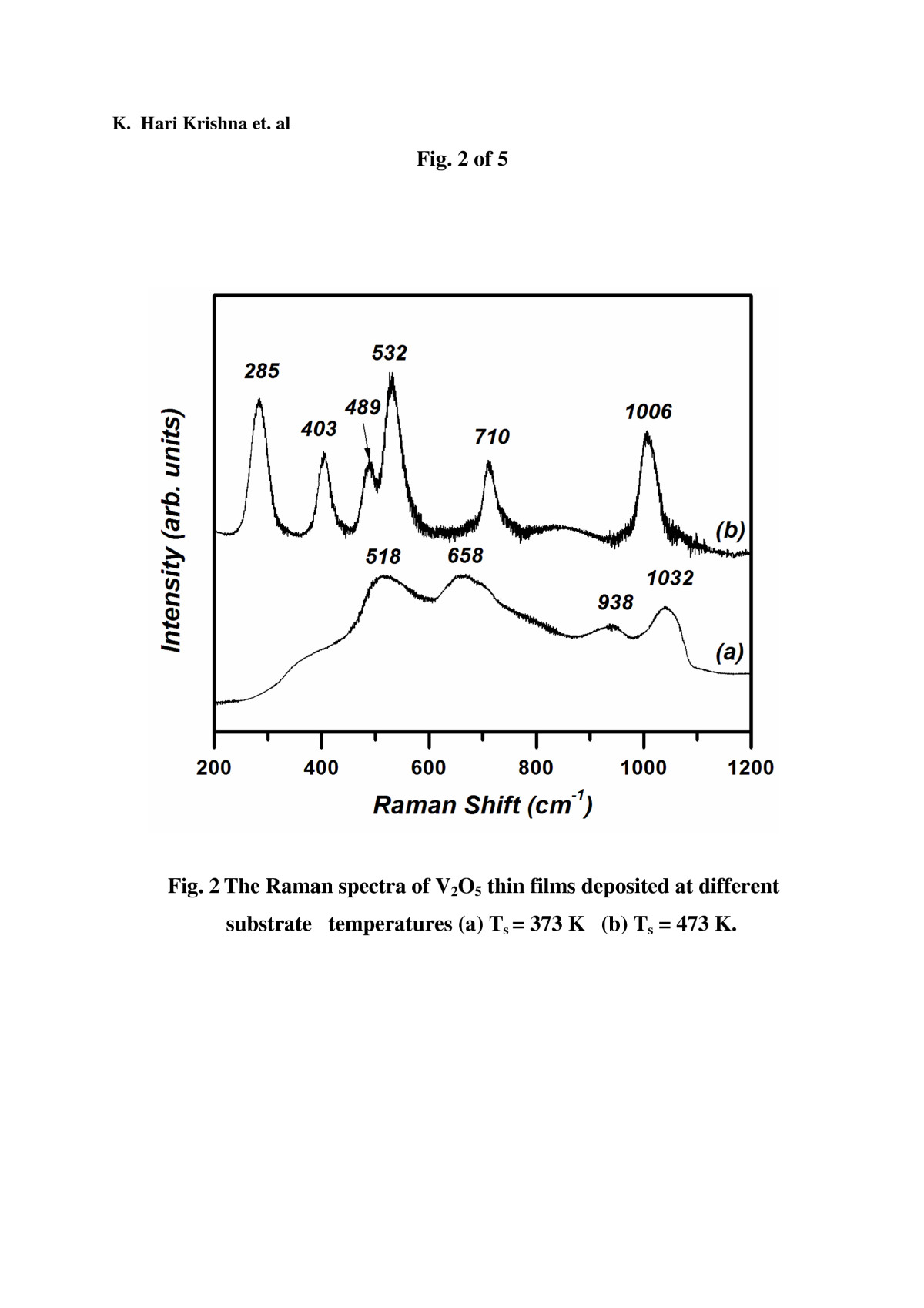
films grown on flexible substrates, as shown in Figure
2
. The broad and non-characteristic Raman spectrum revealed the amorphous nature of V
2
O
5
films deposited at
Ts
< 423 K (Figure
2
curve a). The Raman spectrum of films grown at
Ts
= 473 K exhibited distinguishable and relatively broad characteristic Raman peaks by indicating the nano-crystalline nature of the films (Figure
2
curve b). The spectrum consists of two groups of peaks located at high-frequency region (internal modes), which correspond to stretching and bending of V-O bonds, and at low-frequency region (external modes), which can be viewed as relative motions of structural units with respect to each other. The high-frequency Raman peak at 1,006 cm
−1
corresponds to the vanadyl mode terminal oxygen stretching mode, which results from an unshared oxygen[
23
]. The second peak at 710 cm
−1
is assigned to the doubly coordinated oxygen (V
2
-O) stretching mode which results from corner-shared oxygens common to two pyramids. The third peak at 532 cm
−1
is assigned to the triply coordinated oxygen (V
3
-O) stretching mode which results from edged-shared oxygens common to three pyramids. The two peaks located at 403 and 285 cm
−1
are assigned to the bending vibration of the V=O bonds. The peak located at 489 cm
−1
is assigned to the bending vibrations of the bridging V-O-V (doubly coordinated oxygen) and V
3
-O (triply coordinated oxygen) bonds[
24
]. The well-resolved vanadyl mode present at 1,006 cm
−1
gives the structural quality of the films and can be attributed to the stretching mode related to the
Ag
symmetry vibrations of the shortest vanadium oxygen bond (V=O)[
25
].
Figure 2
The Raman spectra of V2O5thin films deposited at different substrate temperatures.
(curve a)
Ts
= 373 K and (curve b)
Ts
= 473 K.
Surface morphological studies
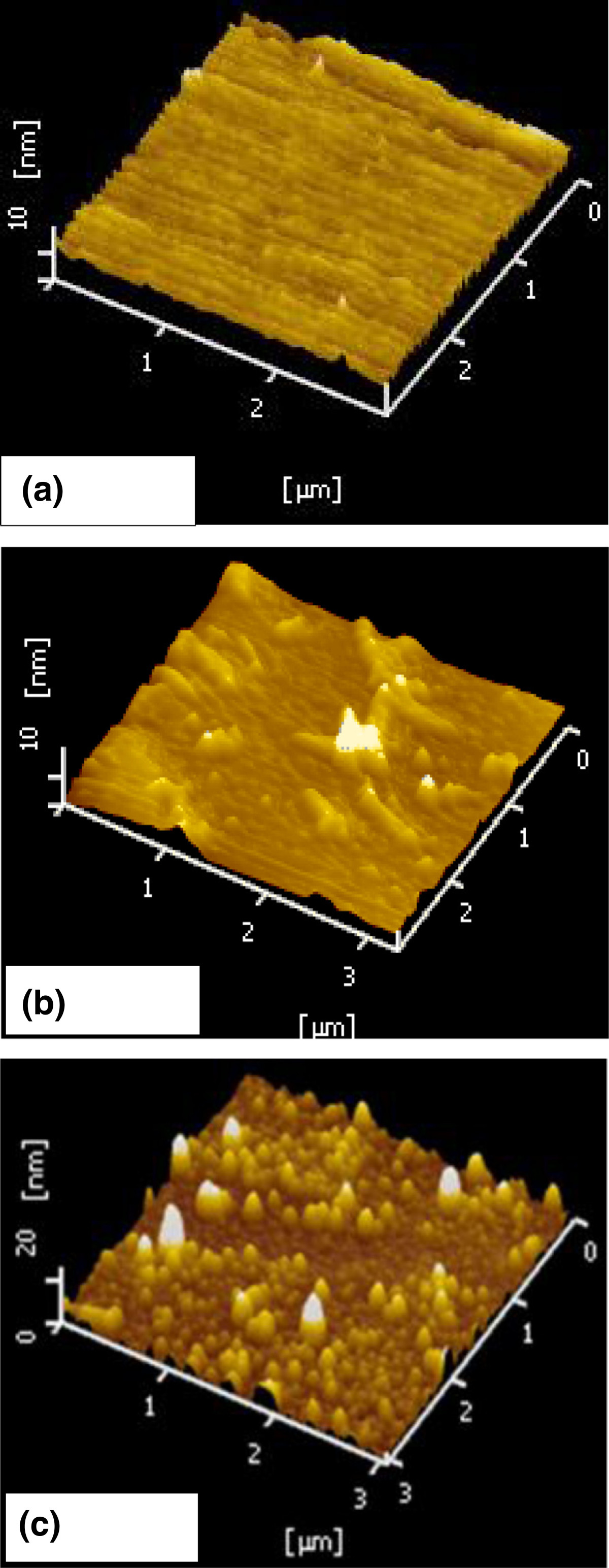
The characteristic changes in surface morphological features of grown films on flexible substrates as a function of substrate temperature is shown in Figure
3
. We observed significant changes in surface topography of the films deposited on flexible substrates, in comparison to films frown on solid substrates. Ramana et al.[
26
] reported surface morphology composed of large rectangular-shaped grains for pulsed laser-deposited V
2
O
5
thin films prepared on silicon substrates, Fateh et al.[
27
] reported surface morphology characterised by small plates for reactive magnetron-sputtered V
2
O
5
thin films, and Luo et al.[
28
] reported grains with tips that grow vertical to the glass substrate for DC magnetron-sputtered V
2
O
5
thin films. In the present investigation, the smooth and featureless AFM surface morphological image (Figure
3
a) of the films grown at
Ts
= 373 K revealed the amorphous nature of the films. However, the uniform ribbon-like structure of layers along the
c
-axis direction and perpendicular to the substrate surface has been observed from AFM studies. At lower substrate temperatures, the rate of coalescence of crystallites is less than the formation of growth centres and favours for vertical growth. Thus, with the enhancement of substrate temperature (>423 K), the adatom mobility is observed to be increased and favours the phenomenon of coalescence to grow vertical grains over the surface face of the films, as evidenced in Figure
3
b. The characteristic change in size and shape of the grains is observed as a function of substrate temperature of flexible substrates above 423 K. The evaporated species interact with the established plasma, reach the surface of the substrates maintained at higher substrate temperatures (
Ts
= 473 K) and acquire larger thermal energy and mobility. This process leads to the enrichment of the diffusion distance, initiates the nucleation and increases the island formation in order to grow continuous film. The surface of the V
2
O
5
films grown at
Ts
= 473 K was observed to be composed of nearly vertical elliptical-shaped nano-sized grains with the size of 98 nm (Figure
3
c) distributed uniformly over the surface of the film provided with root mean square (rms) roughness of 9 nm.
Figure 3
Atomic force micrograms of ARE V2O5thin films deposited at various substrate temperatures on flexible substrates.
(
a
)
Ts
= 373 K, (
b
)
Ts
= 423 K and (
c
)
Ts
= 473 K.
Optical properties
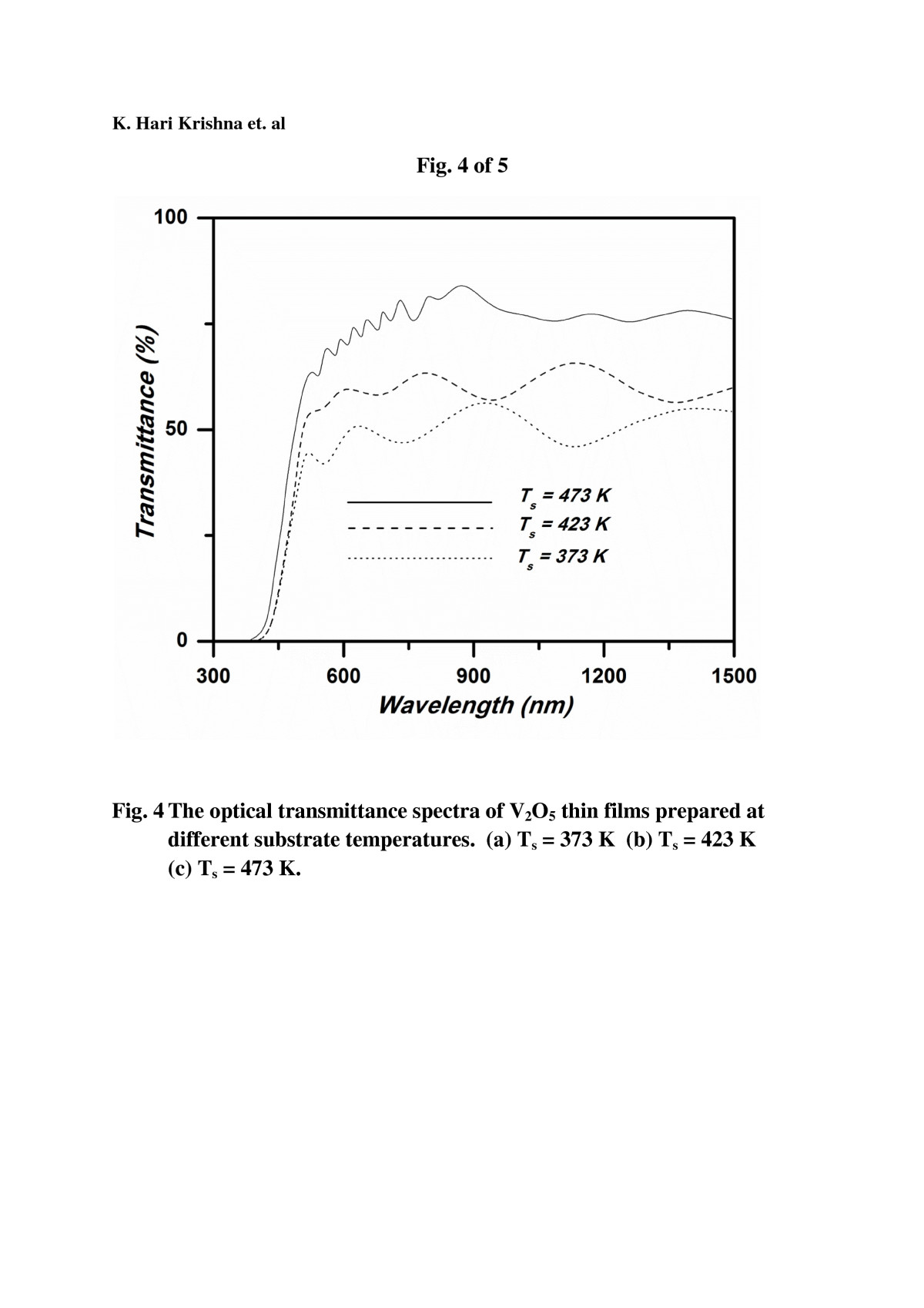
Figure
4
shows optical transmittance spectra recorded in the wavelength range of 300 to 1,500 nm for ARE V
2
O
5
thin films grown on flexible Kapton substrates at various substrate temperatures. The amorphous V
2
O
5
films (deposited at
Ts
= 373 K) demonstrated optical transmittance of 50% throughout the optical transmittance spectrum in the visible region (Figure
4
dotted line), and the sharp optical absorption edge is observed at 450 nm. Increase in optical transmittance in the films is observed with enhancement of substrate temperature to the higher values. Significantly,
blue shift in optical absorption edge and improvement in density of ripples
in the wavelength region of 450 to 750 nm were observed with the rise in substrate temperature from 423 to 473 K. The nano-crystalline V
2
O
5
thin films prepared at
Ts
= 473 K demonstrated an average optical transmittance of 75% in the visible region and observed increased density of ripples in the wavelength region of 450 to 700 nm. Kumar et al. reported 60% of optical transmittance in the visible region for the conventionally evaporated V
2
O
5
thin films grown on amorphous solid glass substrates maintained at 523 K, Avellaneda et al.[
29
] observed 75% of optical transmittance for sol–gel dip-coated V
2
O
5
films on ITO-coated glass substrates, and Lin et al.[
30
] reported average optical transmittance of about 85% in the visible region for reactively sputtered V
2
O
5 −
z
thin films deposited on flexible positron emission tomography (PET)/ITO-coated substrates maintained at room temperature. In the present investigation, nano-crystalline V
2
O
5
films demonstrated appreciable optical transmittance in the visible region, which is consistent with radio frequency (RF)-sputtered films grown on solid substrates. The optical absorption coefficient (
α
) of the grown films is evaluated from standard relations, and the experimentally measured optical absorption coefficient for V
2
O
5
films is found to give better fit to the relation (
α
hν)
2/3
=
A
(hν −
Eg
), where hν is the energy of the incident photon,
B
the absorption edge with parameter and
Eg
the optical bandgap in the visible region with a sharp fall in transmittance in the wavelength region of 400 to 500 nm corresponding to the fundamental absorption edge. The evaluated optical bandgap and refractive indices of the grown films increased as a function of substrate temperature. For amorphous films (
Ts
= 373 K), the evaluated optical bandgap and refractive index values were in the order of 2.31 and 2.28 eV and increased to 2.38 and 2.37 eV, respectively, with the augmentation of substrate temperature to the higher value of 473 K. This small broadening of the bandgap as a function of substrate temperature can be attributed to quantum size effects. Generally, nano-crystalline films composed of low nano-scale-sized grains possess grain boundaries and imperfections, which lead to larger free carrier concentrations and the existence of potential barriers. The electric fields arising from these factors in the disordered state result in an increase in the optical bandgap. Consequently, the observed slight increase of the optical bandgap can be related to the imperfections and grain boundaries in the nano-scale grained structure of V
2
O
5
thin films. The electrochromic performance of deposited V
2
O
5
thin films is significantly influenced by the relative density and porosity of the films, which, in turn, depends upon the refractive index of the films. In general, the density of oxide thin films depends strongly on the film deposition parameters, which can tailor the relative packing density value of the films. Here, the relative packing density of the metal oxide thin films is defined as the relative density to ideally packed bulk vanadium pentoxide with
ρbulk
= 3.36 g/cm
3
. To compare the results quantitatively, the relative packing density of the films is calculated using Lorentz-Lorentz relation expressed as follows:
n2−1/n2+2=Nαp/3∞ε0ρ,
where
n
,
N
,
αp
,
∞
,
ε0
and
ρ
are refractive index, number of dipoles per unit volume, polarizability of dipoles, permittivity of free space and film density, respectively. In parallel, the porosity in the grown films is calculated from estimated refractive index values using first-order rule of mixtures, according to the following equation:
1−XnTD+Xnair=nmeans,
where
X
is the porosity,
nTD
is the refractive index of the film material (which is considered as 2.4 for bulk V
2
O
5
),
nmeans
is the refractive index of grown V
2
O
5
thin film and
nair
is the refractive of air(which is taken as one). The estimated relative densities of deposited films increased as a function of substrate temperature. The amorphous V
2
O
5
films grown at
Ts
= 373 K exhibited a lower relative density of 0.9619. Evaluated porosity values of grown V
2
O
5
films (as tabulated in Table
1
) are observed to decrease with the enhancement of substrate temperature, and as-deposited nano-crystalline films grown at
Ts
= 473 K exhibited a relatively lower porosity value of 0.02.
Figure 4
The optical transmittance spectra of V2O5thin films prepared at different substrate temperatures.
(Dotted line)
Ts
= 373 K, (dashed line)
Ts
= 423 K and (solid line)
Ts
= 473 K.
Table 1
Estimated optical parameter of grown V2O5nano-crystalline thin films at various substrate temperatures on flexible substrates
Substrate temperature (K)
Transmittance T(%)
Refractive index ( n)
Extinction coefficient ( k)
Relative density
Porosity (nm)
Optical bandgap (eV)
373
50
2.28
0.1254
0.9619
0.09
2.31
423
62
2.33
0.0880
0.9784
0.05
2.32
473
75
2.37
0.0559
0.9909
0.02
2.38
Electrochromic properties
The electrochromic properties of grown films were investigated by dry lithiation method. In this method, LiNbO
3
powder was heat-treated at 1,113 K under high vacuum to give off lithium atoms for insertion in the exposed V
2
O
5
films. The quartz crystal monitor was used for the measurement of the film thickness during lithiation process control and calibrated the thickness of the deposited LiNbO
3
film against the electrochemical insertion. In the present investigation, 20-nm effective mass thickness of lithium layer is considered for maximum coloration, which corresponds to approximately 12.5 mC/cm
2
as verified from the electrochemical method. The electrochromic performance of the deposited films was estimated in terms of optical modulation (Δ
T
%), optical density (OD) and the coloration efficiency (
η
) (change in optical density (ΔOD) per unit inserted charge (
Q
)) of grown V
2
O
5
films, which were estimated using the following equations, respectively:
ΔT%=Tbleached%−Tcoloured%,ΔOD=logTbleached%/Tcoloured%,η=ΔOD/Q,
where
Tbleached
(%) is the transmittance of the sample in the bleached state (ion extraction state),
Tcoloured
(%) is the transmittance of the sample in the coloured state (ion insertion state) and
Q
is the charge insertion/extraction per unit area.
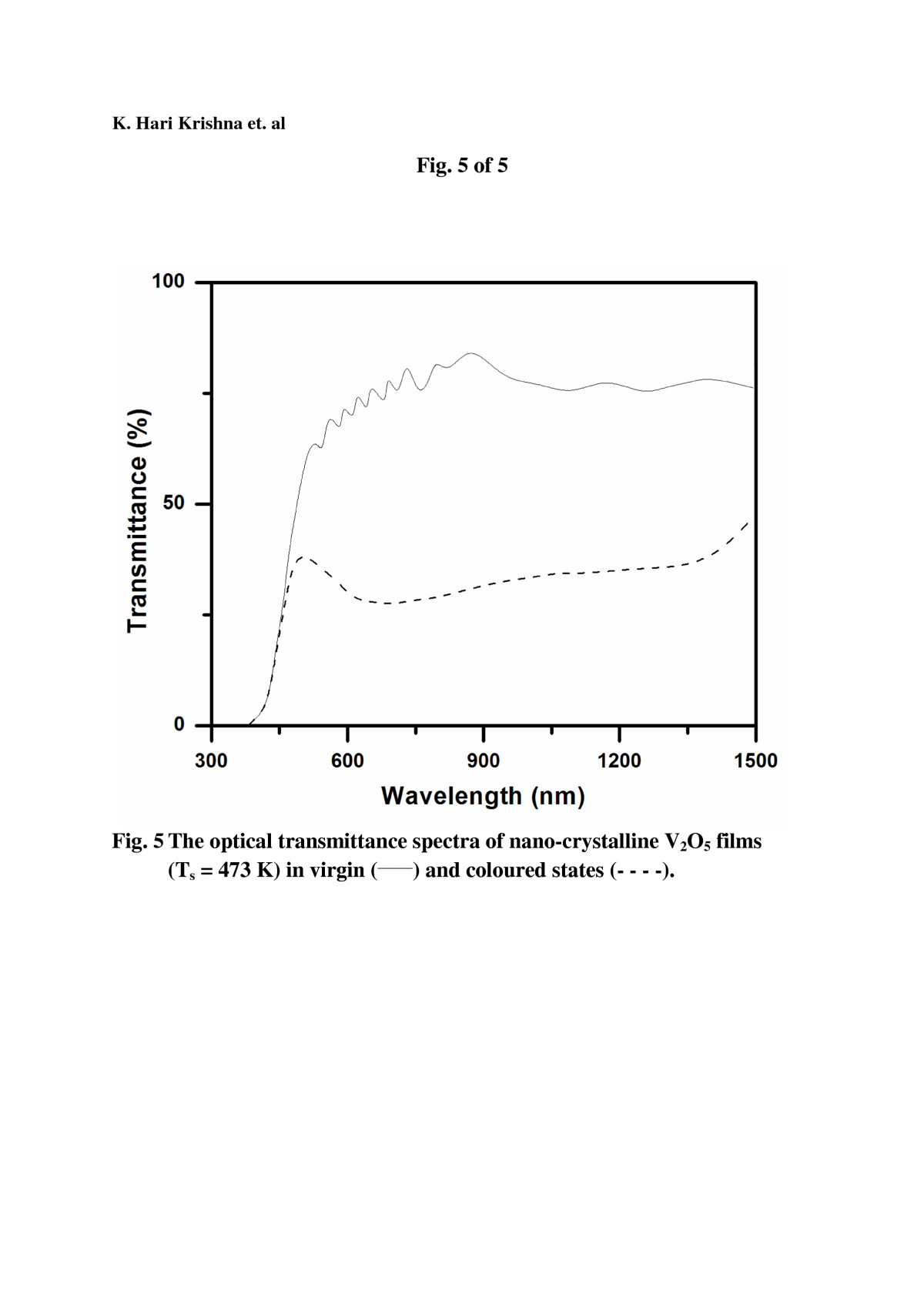
The estimated coloration efficiency of the deposited films was noticed to increase as a function of substrate temperature. The as-deposited nano-crystalline V
2
O
5
films grown on ITO-coated flexible Kapton substrate maintained at
Ts
= 473 K demonstrated better optical modulation of about 36.1% with an estimated coloration efficiency of 26.2 cm
2
/C at a wavelength of 550 nm, as evidenced in Figure
5
. Generally, in nano-crystalline V
2
O
5
films, the optical modulation may occur due to ‘absorption modulation’. The optical absorption is caused by small polaron transitions between two non-equivalent sites of vanadium (V
4+
and V
5+
). Therefore, the inserted electrons are located in V
4+
sites and polarise their surrounding lattice to form small polarons. When the absorption of a photon of appropriate energy occurs by the self-trapped carrier (electron), it can be freed from the potential well which self-traps the electrons. As a result, the electrons excite from the lower energy states (V
4+
) to neighbouring higher energy states (V
5+
). The coloration mechanism in coloured dry-lithiated nano-crystalline V
2
O
5
thin films can be expressed as follows:
V2O5+xLi+xe−↔LixV2O5V5++V5++e−→V4++V5+V4++V5++hν→V5++V4+
Figure 5
The optical transmittance spectra of nano-crystalline V2O5films.Ts
= 473 K in virgin (solid line) and coloured states (dashed line).
Lin et al.[
30
] reported an optical modulation of 36.5% and coloration efficiency of 33.7 cm
2
/C at a wavelength of 400 nm for reactively sputtered thin films of V
2
O
5 −
z
at a room temperature of 23°C on flexible PET/ITO substrates.
Electrochemical properties
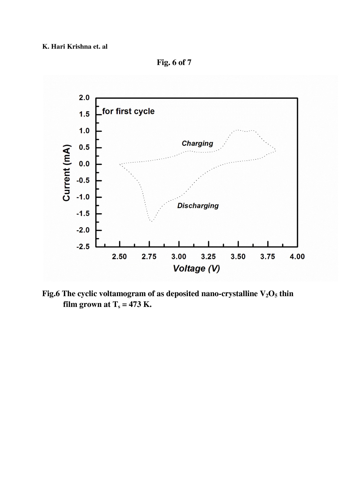
Figure
6
displays cyclic voltammogram (CV) recorded for the as-deposited V
2
O
5
thin films cycled between 4.0 and 2.5 V at a constant scan rate of 10 mV/s. The CV of the grown pure V
2
O
5
film demonstrated two distinguishable broad peaks during charging and discharging processes, which were described as follows[
31
]:
α−V2O5+0.5Li+↔ε−Li0.5V2O5,ε−Li0.5V2O5+0.5Li+↔δ−LiV2O5.
Figure 6
The cyclic voltammogram of as-deposited nano-crystalline V2O5thin film grown atTs= 473 K.
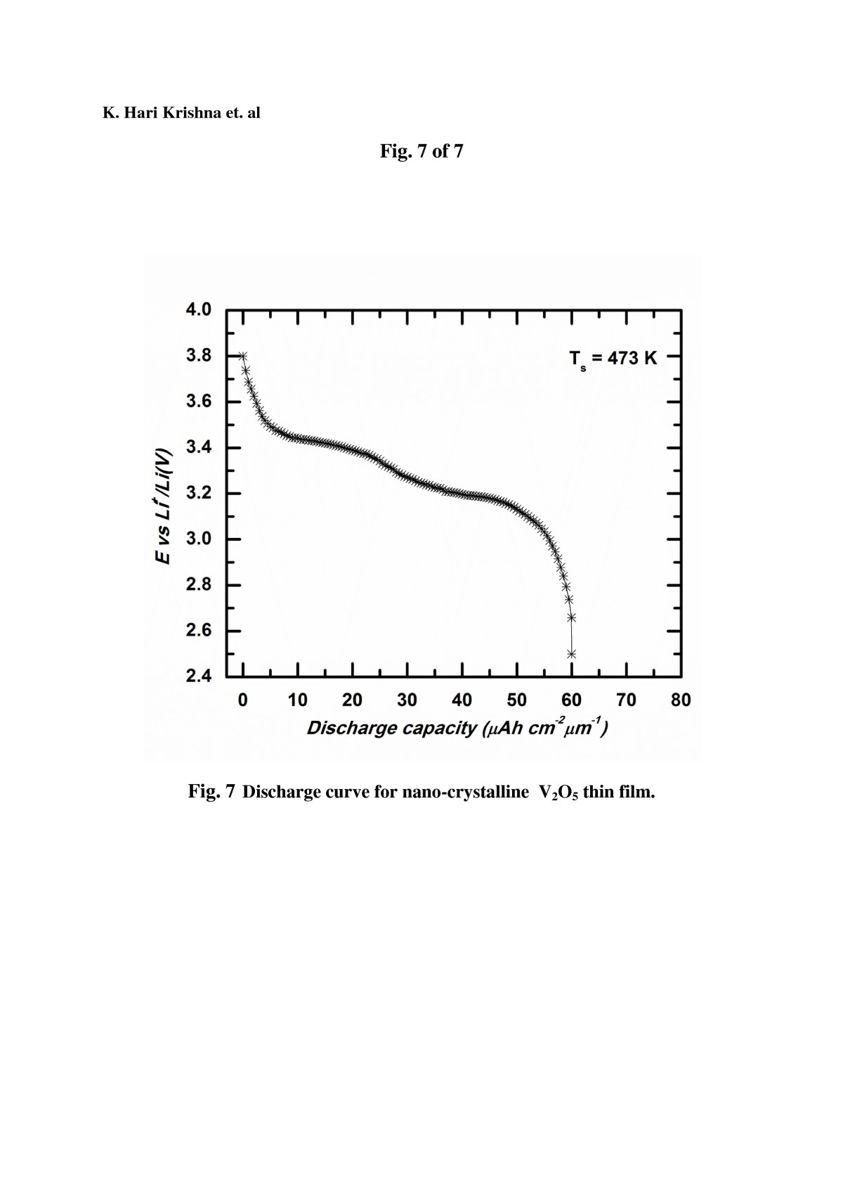
The discharging profile of pure V
2
O
5
films exhibited two plateau regions (Figure
7
) and showed a discharging capacity of approximately 60 μAh cm
−2
μm
−1
. The obtained preliminary electrochemical investigations of as-deposited ARE V
2
O
5
thin films with the thickness of 350 nm deposited on flexible substrates are encouraging and demonstrating relatively less electrochemical performance in comparison with V
2
O
5
films deposited on solid substrates. This may be due to low conductivity of as-deposited V
2
O
5
films, and in general, metal oxide thin films grown on flexible substrates comprise more compressional stresses, which may not favour for easy volume expansion/contraction of the host V
2
O
5
matrix during Li-ion intercalation/deintercalation processes. The investigations are in progress to check cyclic ability of grown films.
Figure 7
Discharge curve for nano-crystalline V2O5thin film.
Conclusions
The nano-crystalline V
2
O
5
thin films were successfully grown on ITO-coated flexible Kapton substrates maintained at 473 K, using home-built activated reactive evaporation technique by employing nano-crystallineV
2
O
5
powder synthesised via co-precipitation method. The X-ray diffraction pattern of grown nano-crystalline films displayed relatively broad and characteristic Bragg reflection of (001) by indicating the
c
-axis growth on flexible substrates. The broad and characteristic Raman peaks revealed the presence of nano-crystalline V
2
O
5
phase in the films. The surface of the as-deposited nano-crystalline films was observed to be composed of vertical elliptical-shaped nano-sized grains with the size of 98 nm and rms roughness of 9 nm, as evidenced in the AFM results. The nano-crystalline V
2
O
5
films demonstrated a relatively higher optical transmittance of 75% in the visible region with an estimated optical bandgap value of 2.38 eV. The evaluated relative density and porosity values for as-deposited nano-crystalline V
2
O
5
films were in the order of 0.09 and 0.02 nm, respectively. The dry-lithiated nano-crystalline films demonstrated better optical modulation of 36.1% and coloration efficiency of 26.2 cm
2
/C at a wavelength of 550 nm. In the present investigation, the obtained results were observed to be encouraging, and they were comparable to previously reported RF-sputtered V
2
O
5
thin films.
Authors' information
KHK obtained his Ph.D. degree from Sri Venkateswara University, India. During his doctorate degree, he worked on ‘growth of metal oxide thin films for the application of Energy conversion and Storage devices’. Later, he joined as a postdoctoral fellow in the Department of Physics, University of Calabria, Italy. Currently, he is continuing his research on ‘growth of pure and nano-composite conducting polymer thin films’. OMH has recived M.Sc. and Ph.D. degrees in Physics from Sri Venkateswara University, Tirupati, India in 1984 and 1990, respectively, and latter worked as a postdoctoral fellow in Universite Pierre et Marie Curie, Paris during 1991–1992. He joined as faculty member in Department of Physics, Sri Venkateswara University in 1992 and currently working as professor. So far, he has guided nine Ph.D. students and seven M.Phil. students and published 120 research articles in peer reviewed journals. His current research interest is on growth and characterization of poly- and nano-crystalline metal oxide thin films for electrochemical, electrochromic and sensor applications. GC is a senior researcher at the Department of Energy, CIEMAT, belonging to the Spanish Ministry of Economy and Competitiveness. GC received a Ph.D. in Applied Physics, and his topics of interest are the preparation and characterization of thin-film semiconductor materials for solar cells and other optoelectronic devices.
Acknowledgements
The authors highly acknowledge M. Mohan Rao, scientist, Indian Institute of Chemical Technology, Hyderabad, for his valuable suggestions to carry out the experiments to synthesize nano-crystalline V
2
O
5
powder.
Competing interests
The authors declare that they have no competing interests.
Authors' contributions
GC provided radio frequency (RF)-sputtered indium tin oxide-coated Kapton substrates to carry out further steps in the present work. KHK designed the activated reactive evaporation technique and optimized the growth conditions to prepare V
2
O
5
thin film on flexible substrates. He carried out all the characterizations and interpreted the results under guidance of OMH. OMH has assisted during electrochemical characterization and guided to present the current research work in a fruitful way. All authors read and approved the final manuscript.
References
Cogan et al. (1987) Solar modulation in a-WO3/a-IrO2 and c-KxWO3+(x/2)/a-IrO2 (pp. 371-382) 10.1016/0165-1633(87)90031-1
Anderson et al. (1989) Electrochromic LixWO3/polymer laminate/LiyV2O5 (pp. 3295-3308) 10.1364/AO.28.003295
Lampert et al. (1999) Durability evaluation electrochromic devices: an industry perspective (pp. 449-463) 10.1016/S0927-0248(98)00185-8
Granqvist et al. (2003) Electrochromic coatings and devices: survey of some recent advances (pp. 201-211) 10.1016/S0040-6090(03)00983-0
Somani and Radhakrishnan (2002) Electrochromic materials and devices: present and future (pp. 117-133) 10.1016/S0254-0584(01)00575-2
Lampert (1984) Electrochromic materials and devices for energy efficient windows (pp. 1-27) 10.1016/0165-1633(84)90024-8
Cogan et al. (1989) Optical properties of electrochromic vanadium pentaoxide (pp. 1333-1337) 10.1063/1.344432
Nadkarni and Shirodkar (1983) Experiment and theory for switching in Al/V2O5/Al devices (pp. 115-129) 10.1016/0040-6090(83)90200-6
Lee et al. (2003) Raman spectroscopic studies of amorphous vanadium oxide thin films (pp. 111-116) 10.1016/j.ssi.2003.08.022
Park et al. (2002) Electrochemical properties of vanadium oxide thin film deposited by r.f. sputtering (pp. 229-235) 10.1016/S0167-2738(02)00437-X
Baddour-Hadjean et al. (2009) In situ Raman microspectrometry investigation of electrochemical lithium intercalation into crystalline V2O5 thin films (pp. 6674-6679) 10.1016/j.electacta.2009.06.052
Ramana et al. (1997) Growth and structure of electron beam evaporated V2O5 thin films (pp. 195-199) 10.1016/S0254-0584(97)01914-7
Han et al. (2008) Improved conductivity and mechanism of carrier transport in zinc oxide in with embedded silver layer10.1063/1.2829788
Srinivasa Rao et al. (2003) Photochromic properties of double layer CdS/MoO3 nano-structured films (pp. 79-86) 10.1016/S0921-5107(03)00078-3
Hari Krishna et al. (2008) Photo- and electrochromic properties of activated reactive evaporated MoO3 thin films grown on flexible substrates (pp. 1-5) 10.1155/2008/217510
Jayalakshimi et al. (2007) Hydrothermal synthesis of SnO2-V2O5 mixed oxide and electrochemical screening of carbon nano-tubes (CNT), V2O5, V2O5-CNT and SnO2-V2O5-CNT electrodes for super capacitors (pp. 578-583) 10.1016/j.jpowsour.2006.11.025
Hari Krishna et al. (2010) Electrochromic properties of nanocrystalline WO3 thin films grown on flexible substrates by plasma-assisted evaporation technique (pp. 921-929) 10.1007/s00339-010-5681-5
Beydaghyan et al. (2008) Electrochromic and morphological investigation of dry-lithiated nanostructured tungsten trioxide thin films (pp. 1646-1650) 10.1016/j.tsf.2007.05.006
Aita et al. (1986) Optical behaviour of sputter-deposited vanadium pentoxide (pp. 749-753) 10.1063/1.337425
Julien et al. (1995) The growth of V2O5 flash evaporated films (pp. 934-936) 10.1007/BF02427469
Ramana et al. (1998) Influence of oxygen partial pressure on the optical properties of electron beam evaporated vanadium pentaoxide thin films (pp. 101-107) 10.1016/S0925-3467(97)00168-7
Abello et al. (1983) Vibrational spectra and valence force field of crystalline V2O5 (pp. 641-651) 10.1016/0584-8539(83)80040-3
Ramana et al. (2003) Microstructural features of pulsed laser deposited V2O5 thin films (pp. 135-138) 10.1016/S0169-4332(02)01411-3
Fatch et al. (2008) Synthesis and structure relations for reactive magnetron sputtered V2O5 films (pp. 1551-1555) 10.1016/j.surfcoat.2007.07.010
Luo et al. (2010) Impact of substrate temperature on microstructure, electrical and optical properties of sputtered nanocrystalline V2O5 thin films (pp. 145-150) 10.1016/j.vacuum.2010.05.001
Avellaneda and Bulhões (2006) Optical and electrochemical properties of V2O5:Ta sol–gel thin films (pp. 444-451) 10.1016/j.solmat.2005.04.031
Lin et al. (2008) Electrochromic properties of V2O5−z thin films sputtered onto flexible PET/ITO substrates (pp. 290-297) 10.1016/j.ssi.2008.01.054
Ng et al. (2009) Flame spray pyrolyzed vanadium oxide nanoparticles for lithium battery cathodes (pp. 3748-3755) 10.1039/b821389p