Nanomaterials Research Laboratory, Department of Physics, G. D. M. Arts, K. R. N. Commerce and M.D. Science College, Jamner, Maharashtra, 424 206, IN
Department of Physics, Arts, Commerce and Science College, Bodwad, Maharashtra, 425 310, IN
Abstract
Nanostructured copper oxide (CuO) thin films were prepared by spray pyrolysis technique. X-ray diffraction was used to investigate the structural properties. Surface morphology was studied using scanning electron microscopy. Microstructure was studied using a transmission electron microscope, and energy-dispersive X-ray analysis was used to determine the elemental composition of prepared nanostructured CuO thin film. Gas-sensing performance was conducted using static gas-sensing system, at different operating temperatures in the range of 200°C to 400°C for the gas concentration of 100 ppm. The maximum sensitivity (
S
= 872) to H
2
S was found at the temperature of 250°C. Quick response (2 s) and fast recovery (5 s) are the main features of this film.
Background
Metal-oxide semiconductor chemical sensors have been a subject of intensive research due to their industrial and domestic applications in toxic and flammable gas detection. Because of an increasing demand for fast and continuous detection, current research in gas sensor techniques has been focused on the development of sensors which have the characteristics of low cost, rapid response, high sensitivity, and good selectivity [
1
,
2
].
Copper oxide (CuO) is a p-type semiconductor with a bandgap of 1.5 to 1.8 eV. Copper oxide has been employed in heterogeneous catalysis for several environmental processes as well as in the production of gas-sensing devices, owing to the conductivity changes induced by the reaction of gases with surface-adsorbed oxygen. The addition of small amounts of additives is known to provide better sensitivity [
3
–
7
].
Hydrogen sulfide (H
2
S) is a toxic and inflammable gas, produced in sewage plants, coal mines, and oil and natural gas industries. It is used in large amounts in various chemical industries, research laboratories, and as a process gas in the production of heavy water [
8
].
Spray pyrolysis technique competes with other techniques due to its low cost, suitable properties, and process well suited to large-scale production. In this work, nanostructured CuO thin films with different spraying time of the solution were prepared by spray pyrolysis technique. Crystal structure and grain sizes were studied from X-ray diffraction, scanning electron microscopy (SEM), and transmission electron microscopy (TEM). Elemental composition was carried out using energy-dispersive X-ray analysis (EDAX). These nanostructured CuO thin films were tested for sensing different conventional gases and were observed to be most sensitive to H
2
S at 250°C.
Methods
Experimental
Preparation of nanostructured CuO thin films
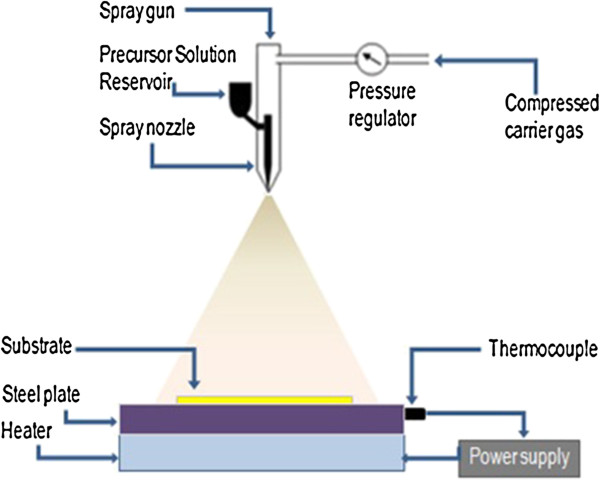
Copper oxide thin films were prepared using spray pyrolysis technique as shown in Figure
1
. The films were deposited by varying the deposition time of solution between 10 to 40 min. The solution was prepared by dissolving copper chloride dehydrate (CuCl
2
.2H
2
O) (RANKEM) in deionized water. The spray produced by a nozzle was sprayed onto the glass substrates heated at 250 ± 5°C.
Figure 1
Spray pyrolysis technique.
Various parameters such as solution concentration (0.05 M), spray rate (8 mL/min), nozzle to-and-fro frequency (15 cycles/min), nozzle-to-substrate distance (30 cm), etc. were optimized to obtain good-quality films. This resulted in the formation of well-adherent and uniform nanostructured copper oxide thin films. The films with different deposition times of 10, 20, 30, and 40 min were obtained and were referred to as S1, S2, S3, and S4, respectively. The samples were fired at 500°C for 1 h.
Sensing system for the measurement of gas response
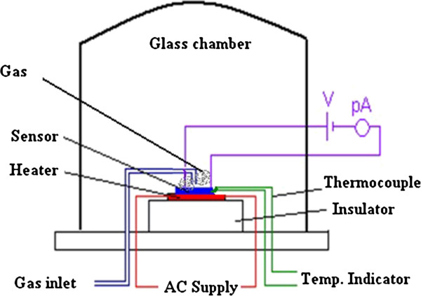
Figure
2
shows a gas-sensing system. The gas-sensing studies were carried out using a static gas chamber to sense H
2
S gas in air ambient. The nanostructured CuO thin films were used as the sensing elements. A Cr-Al (chromel-alumel) thermocouple is mounted to measure the temperature. The output of the thermocouple is connected to a temperature indicator. A gas inlet valve was fitted at one of the ports of the base plate. Gas concentration inside the static system is achieved by injecting a known volume of test gas in the gas-injecting syringe. Constant voltage is applied to the sensor, and current can be measured by a picoammeter.
Figure 2
Gas-sensing system.
Characterizations of thin films
The nanostructured CuO thin films were characterized by X-ray diffraction (Miniflex Model, Rigaku, Tokyo, Japan) using CuK
α
radiation with a wavelength of
λ
= 1.5418 Å. The microstructure and element composition of the films was analyzed using a scanning electron microscope coupled with a energy-dispersive spectrophotometer (JEOL 2300 model, Tokyo, Japan) and TEM (CM 200 Philips, Amsterdam, Netherlands (200 kV HT)). Gas-sensing properties were measured using a static gas-sensing system. The sensor performance on exposure to liquefied petroleum gas (LPG), carbon dioxide, hydrogen, ammonia, ethanol, chlorine, and H
2
S was examined.
Results
Structural properties
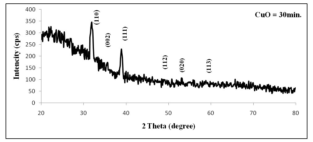
The structural characterization of nanostructured CuO thin films was made by X-ray diffraction technique with monochromatic CuKα radiation, λ = 1.5418Å. Figure
3
shows the X-ray diffractogram of the most sensitive film (sample S3). The observed peaks, (110) (002), (111), (112), (020), and (113), are very well matched with the JCPDS data of CuO (ASTM card no. 80-1917). The average crystalline size calculated from Scherrer’s formula was found to be 29 nm.
Figure 3
X-ray diffractogram of the most sensitive nanostructured CuO thin film (sample S3).
Microstructure study
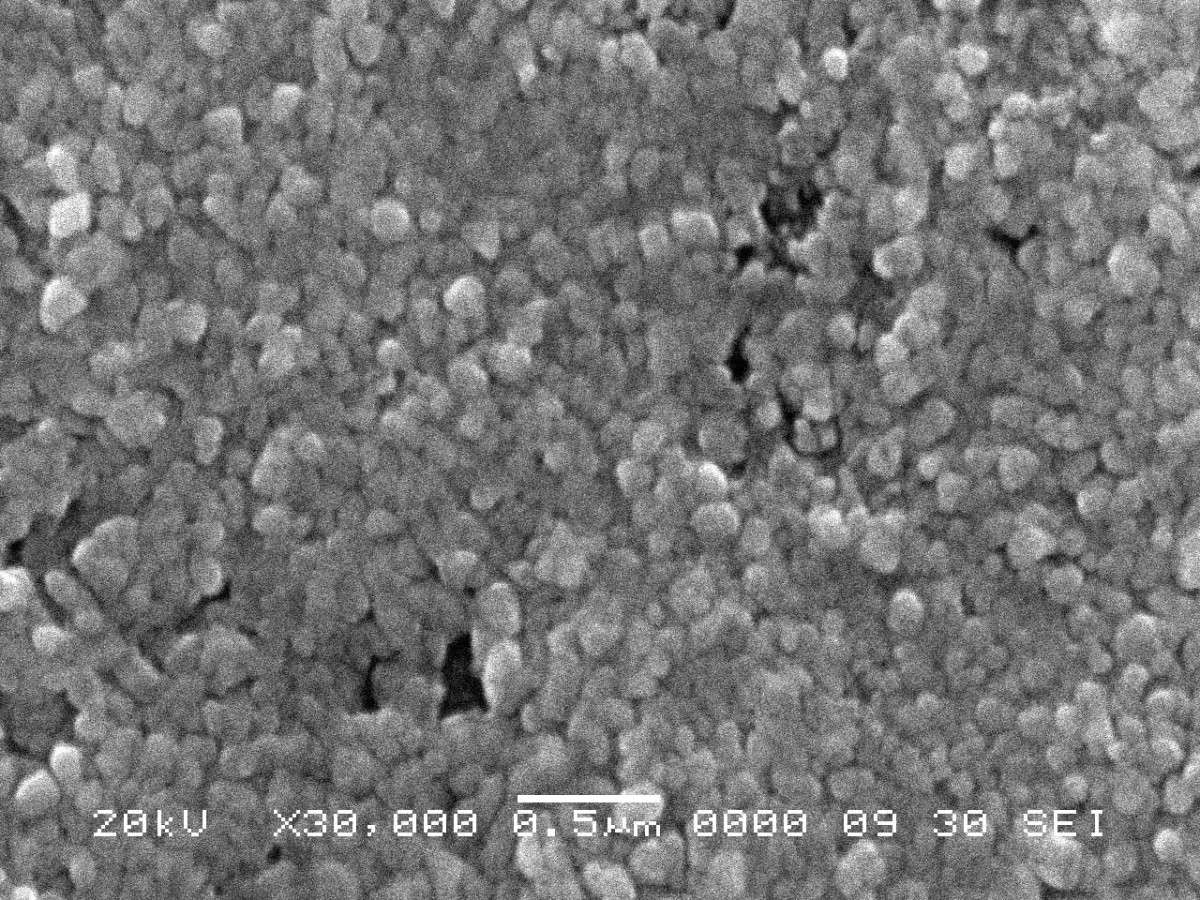
Surface topography of the films was analyzed using scanning electron microscopy, as shown in Figure
4
. The morphology of the particles was roughly spherical in shape. The average grain size was about 30 nm.
Figure 4
SEM images of the most sensitive nanostructured CuO thin film (sample S3).
Transmission electron microscopy
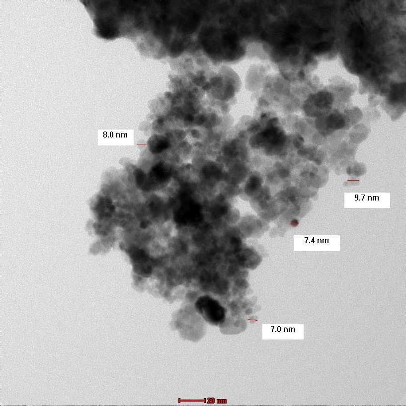
Figure
5
shows the transmission electron micrograph of the most sensitive nanostructured CuO thin films (sample S3) obtained by scratching the thin film. The powder was dispersed in ethanol. A copper grid was used to hold the powder. It is clear from the TEM image that the grains are nanostructured in nature and nearly spherical in shape, with size smaller than 9 nm.
Figure 5
TEM images of the most sensitive nanostructured CuO thin film (sample S3).
The electron diffraction pattern of sample S3 was shown in Figure
6
. It shows spotty but continuous ring patterns without any additional diffraction spots and rings of secondary phases, revealing their highly crystalline structure.
Figure 6
Electron diffraction pattern of the most sensitive nanostructured CuO thin film (sample S3).
Quantitative element analysis
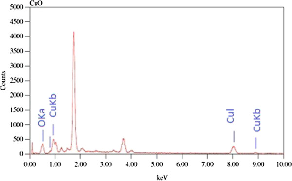
Figure
7
shows the quantitative elemental composition of the most sensitive nanostructured CuO thin film (sample S3) which was analyzed using an energy-dispersive spectrometer. The stoichiometrically expected atomic percentage of Cu and O is 50:50, respectively. The observed atomic percentage of Cu and O is 42.60 at % and 57.40 at %, showing a nonstoichiometric nature.
Figure 7
EDAX of the most sensitive nanostructured CuO thin film (sample S3).
Measurement of sensing parameters
Gas response
It is defined as the change conductance of the sample on exposure to gas to the original conductance. It is given by the relation
S=Gg-GaGa=ΔGG
where
Gg
is the conductance of sensor in gas, and
Ga
is the conductance of sensor in the presence of air.
Selectivity
The response of the sensor to a specific gas in the mixture of gases is the selectivity.
Response time
The time taken by the sensor to attain 80% of the maximum change in resistance on exposure to the gas is the response time.
Recovery time
The time taken by the sensor to roll back to 80% of its original resistance is the recovery time.
Gas-sensing performance
Gas response
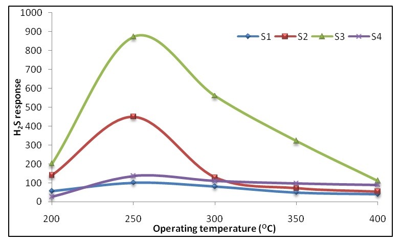
Figure
8
shows variation of gas response with operating temperature of samples S1, S2, S3, and S4 on exposure to 100 ppm of H
2
S. It is clear from Figure
8
that the response of H
2
S goes on increasing with increase in operating temperature, reaches maximum at 250°C, and further decreases with increase in operating temperature. H
2
S response of sample S3 is higher (
S
= 872) at 250°C as compared to those of S1, S2, and S4. It is well known that the sensitivity of metal-oxide semiconductor sensors is mainly determined by the interactions between a target gas and the surface of the sensors [
9
].
Figure 8
Sensitivity of pure nanostructured CuO thin films with operating temperature.
Selectivity
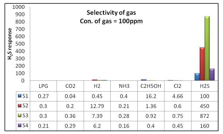
Selectivity of the nanostructured CuO thin film sensors is measured at an operating temperature of 250°C. Figure
9
depicts the bar diagram indicating H
2
S selective ability of the sensor. It is clear from the figure that the responses of all samples to LPG, CO
2
, H
2
, NH
3
, C
2
H
5
OH, and Cl
2
gases are lower as compared to their response to H
2
S.
Figure 9
Selectivity of nanostructured CuO thin films for different gases.
Response and recovery of the sensor
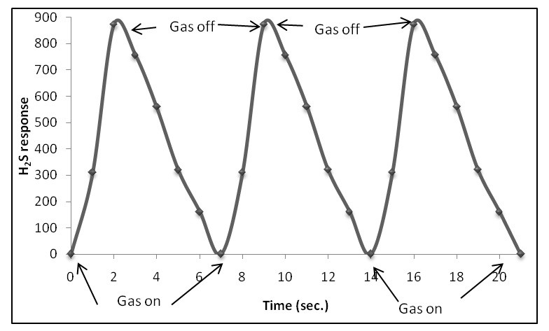
The response and recovery of the most sensitive nanostructured CuO thin film (sample S3) sensor on exposure to 100 ppm of H
2
S at 250°C are represented in Figure
10
. The response is quick (2 s) and recovery is fast (5 s).
Figure 10
Response and recovery of the sensor.
Discussion
Gas-sensing mechanism is based on the amount of oxygen adsorbed (O
2
-, O-, O
2
-) on the sensor surface and is a function of temperature. At the operating temperature, in the absence of a target gas, oxygen gets adsorbed on the surface of the sensor, and it extracts electrons from the conduction band of the sensor material [
10
,
11
]. The amount of oxygen adsorbed on a thin film surface depends on the operating temperature, particle size, and specific surface area of the sensor. The state of oxygen on the surface of CuO thin film undergoes the following reaction:
O2gas→O2adsO2gas+e-→O2-adsO-+e-→O2-ads
The oxygen species capture electrons from the material, which results in the concentration changes of holes or electrons in the CuO semiconductor. When the CuO thin film is exposed to H
2
S gas, the reductive gas reacts with the oxygen adsorbed on the thick film surface. Then the electrons are released back into the semiconductor, resulting in the change in the electrical conductance of CuO thin films. It can be expressed in the following reaction:
H2S+3O→H2O+SO2+6e
Conclusions
Nanostructured CuO thin films could be prepared by a simple and inexpensive chemical spray pyrolysis technique. The structural and microstructural properties confirm that the as-prepared CuO thin films are nanostructured in nature. The element composition of the nanostructured CuO shows a nonstoichiometric nature. The nanostructured CuO thin film of sample S3 was the most sensitive to H
2
S gas and exhibited the response of
S
= 872 to the gas concentration of 100 ppm at the temperature of 250°C. The sensor has good selectivity to H
2
S against LPG, CO
2
, H
2
, NH
3
, ethanol, and Cl
2
. The nanostructured copper oxide thin films exhibit rapid response (2 s) and recovery (5 s).
Authors’ information
RHB is an associate professor and head at the Nanomaterials Research Lab., Department of Physics, G. D. M. Arts, K. R. N. Commerce and M.D. Science College, Jamner. He received an MSc degree in applied electronics and PhD in materials science. His topics of interest are nanomaterials, ceramic gas sensors, photo-conducting and photoluminescent materials, growing crystals, dielectric properties of materials, nanomaterials, and thin and thick film physics. SBP is a research fellow and is working for his PhD at the Nanomaterial Research Lab., Department of Physics at G. D. M. Arts, K. R. N. Commerce and M.D. Science College, Jamner, He received his MSc degree in physics from North Maharashtra University, Jalgaon, in 2007. ARB is an assistant professor and head of the Department of Physics at Arts, Commerce and Science College, Bodwad. He received his MSc degree in physics and PhD degree in nanocrystalline-based gas sensor from North Maharashtra University, Jalgaon. His topics of interest are nanomaterials, gas sensor, chemical warfare agent and their simulant detections, thick and thin film physics, photoconducting and photoluminescent material, and sunscreen lotions.
Acknowledgments
The authors are thankful to the University Grants Commission, New Delhi, for providing financial support. Thanks to Principal, G. D. M. Arts, K. R. N. Commerce and M.D. Science College, Jamner, for providing the laboratory facilities for this work.
Competing interests
The authors declare that they have no competing interests.
Authors’ contributions
RHB, SBP, and ARB contributed equally to this manuscript. All authors readand approved its final version.
References
Patil et al. (2012) Detection of dimethyl methyl phosphonate – a simulant of sarin: the highly toxic chemical warfare – using platinum activated nanocrystalline ZnO thick films (pp. 372-380) 10.1016/j.snb.2011.10.047
Bari et al. (2012) Influence of precursor concentration of solution on CO sensing performance of sprayed nanocrystalline SnO2 thin films (pp. 887-895)
Oritz et al. (2001) A catalytic application of Cu2O and CuO films deposited over fiberglass (pp. 177-184) 10.1016/S0169-4332(00)00822-9