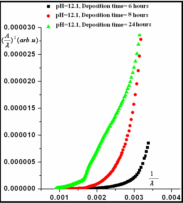
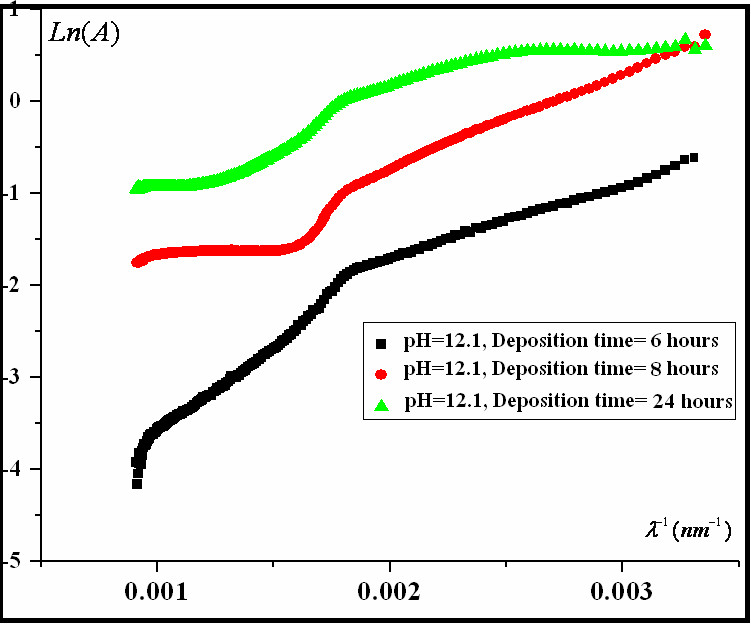
In this article, using the Tauc model, the absorption spectrum fitting method was applied to estimate the optical band gap and width of the band tail of the CdSe nanostructural films that requires only the measurement of the absorbance spectrum, and no additional information such as the film thickness or reflectance spectra is needed. Samples are prepared by chemical bath deposition method. Fabricated nanostructural thin films are thick but are composed from nanoparticles.
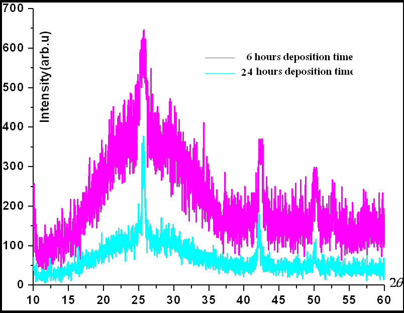
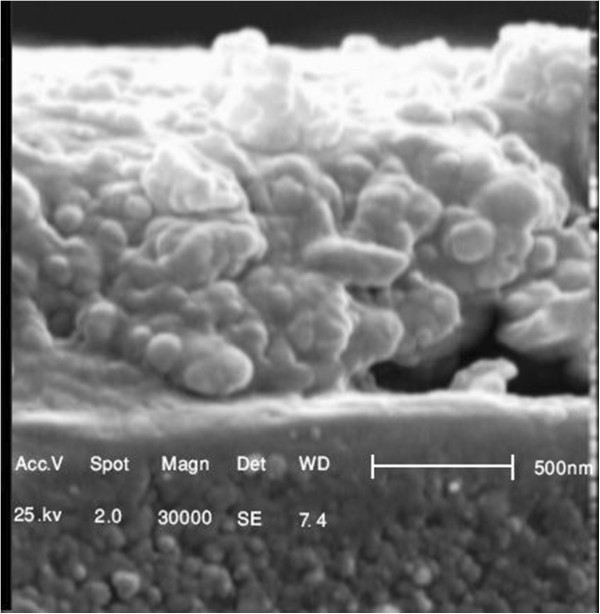
The semiconductor nanoparticles have properties between molecules and bulk solid semiconductors. Their physicochemical properties are found to be strongly size dependent [ 1 – 8 ]. It is well known that the nanoscale systems show interesting physical properties such as increasing semiconductor band gap due to electron confinement [ 8 – 11 ]. Surface atoms play an important role in governing the electronic and optical properties in nanomaterials. The estimation of energy band gap in nanostructural semiconductors is somewhat difficult because surface atoms edges of the valence and conduction bands are not abrupt and the tail states complicate the definition of the true optical gap [ 1 – 8 ]. The aim of this paper is to explain how one can determine the energy band gap in nanostructural semiconductors that only requires the measurement of the absorbance spectrum and without the need of additional information, such as the film thickness or reflectance spectra [ 12 , 13 ]. Cadmium selenide belongs to the binary metal chalcogenides of group A II -B VI semiconductors and is a widely used A II B VI semiconductor where its bulk band gap ( E g = 1.74 eV) lies in the solar energy spectrum. Chemical bath deposition (CBD) method is presently attracting considerable attention as it does not require sophisticated instrumentation. It is relatively inexpensive, easy to handle, convenient for large area deposition, and capable of yielding good quality thin films. The characteristics of the chemically deposited CdSe thin films by CBD strongly depend on the growth condition, and by changing the deposition key parameters one can control thickness, size of nanoparticles, and the energy band gap of the obtained thin films.
Brus considered a model for the energy band gap with particle size that yields the following expression for the band gap,
E
R
, of the quantum dot,
Where E R is the bulk band gap, and R is the radius of the quantum dot; m e , m h , and ε are electron mass, hole mass, and dielectric constant, respectively. The third term arises due to the Coulomb attraction [ 8 – 10 ].
The CdSe thin films were grown on ordinary glass slides (26 × 7.6 × −2 mm). Before deposition, the substrates were washed in detergent, rinsed in acetone, ultrasonically cleaned, and finally rinsed again with a mixture of double distilled water and methanol. The substrates were kept in vacuum. The deposition solution was prepared by a process similar to that used by Mane et al. [ 14 ]. A 400 ml of 0.25 M cadmium acetate (to provide Cd 2+ ions) was taken in a glass beaker with 1,000 ml capacity, under constant stirring, and then 25% ammonia was added to this solution slowly. At first the solution become milky and further addition of excess ammonia made the solution clear and transparent. A 400 ml of freshly prepared 0.25 M Na 2 SeSo 3 [ 14 ] was added slowly to the solution. The glass substrates were vertically immersed in to the deposition solution with volume (12 × 19 × 15 cm), and the bath solution was covered.
In order to control the rate of film growths, the bath temperature was kept constant at desired value (room temperature). In order to control the pH, ammonia is added to the solution which contains Cd 2+ ions. At the end of the deposition process, all the deposited substrates were removed from the chemical bath at suitable intervals (4 to 24 h) and were washed with deionized water and methanol to remove the loosely adhering CdSe nanoparticles on the film. The coating of one side of each substrate was removed by cotton swab moistened with dilute HCl, and then the films were dried in the air and finally placed in the desiccators.
The overall reaction is shown as [
15
]
The films were structurally characterized by X-ray diffraction (XRD) using a Philips Analytical X-ray diffractometer (Royal Philips Electronics, Amsterdam, The Netherlands) in the 2 ⊖ geometry. The optical absorption was measured by a UV–vis spectrometer. Surface morphology was investigated by scanning electron microscopy.
In crystalline semiconductors, the following equation has been obtained to relate the absorption coefficient to incident photon energy [
16
,
17
]:
where
E
gap
, B, and hυ are the optical gap, constant, and incident photon energy, respectively; α(
v
) is the absorption coefficient defined by the Beer-Lambert’s law as
where
λ
g
,
h
, and
c
are wavelengths corresponding to the optical band gap, Planck’s constant, and velocity of light, respectively. Using the Beer-Lambert’s law, it is possible to rewrite Equation
4
as follows:
where
Extrapolating the straight-line portion of the plots shown in Figure
1
to zero
ASF plots for samples with 6-, 8-, and 24-h deposition times.Figure 1

Energy band gap and width of band tail for CdSe nanoparticle films at pH = 12
Samples (deposition time in hours) | ||
|---|---|---|
6 | 3.93 | 1.07 |
8 | 3.58 | 1.05 |
24 | 2.52 | 2.32 |
It has been suggested that the Urbach’s rule may be used to relate the absorption coefficient to the incident photon energy [
12
] as
where
α
0
is a constant and
E
tail
is width of the tail of localized states (Urbach energy) corresponding to the optical transition between localized states adjacent to the valence band and extended state in the conduction band which is lying above the mobility edge. In ASF procedure, Equation
5
can be written as
where
D
3
is (
α
0
d
/2.303). Therefore, the values of
E
tail
, in electron volts, were obtained from the slope of the linear region of the
Plots of Ln (Abs) vs. (1/
λ
) for samples with 6-, 8-, and 24-h deposition times.Figure 2

X-ray diffraction patterns for CBD-CdSe thin films on the glass substrate are shown in Figure
3
. As deposition time is increased, the intensity and the line width of the XRD patterns get higher and smaller, respectively. The obtained results are shown in Table
2
. The samples’ X-ray patterns illustrate that the crystal structure of the CBD-CdSe is cubic [
15
].
(Color online) XRD patterns of samples with 6- and 24-h deposition times.Figure 3

Summary of X-ray characterization of nanoparticle sizes for samples
Sample (at pH = 12.1) | Peak | ( | (2 | (Hkl planes) | |
|---|---|---|---|---|---|
6-hdeposition | 3 | 3.50091 | 1.15 | 25.68 | 111 |
2.14792 | 1.23 | 42.15 | - | ||
1.82922 | 0.62 | 49.94 | - | ||
24-h deposition | 3 | 3.47243 | 0.44 | 25.465 | 111 |
2.14162 | 0.36 | 42.11 | 220 | ||
1.82375 | 0.62 | 49.94 | 311 |
Figure
4
shows the scanning electron microscope (SEM) picture of the 24-h deposition time at pH = 12.1 with magnification × 30,000. It can be observed that the CdSe thin film covers the substrate. From the picture, it is obviously seen that the film is composed of small, nanosized grains. We cut the sample after the deposition. The substrate and sample images are shown separately.
SEM picture of the sample with 24-h deposition.Figure 4

The aim of this paper is to explain how one can determine the energy band gap in nanostructural semiconductors that only requires the measurement of the absorbance spectrum and no additional information is needed, such as the film thickness or reflectance spectra. The cadmium selenide nanoparticle films have been deposited by chemical bath deposition method (CBD). Fabricated nanostructural thin films are composed of small nanosized grains. Using the Tauc model, the absorption spectrum fitting method (ASF) was employed to estimate the optical band gap. Surface atoms in nanostructural semiconductors have a characteristic role. ASF method presents the width of band tail for nanostructural semiconductors.
The author declares that he has no competing interest.