Methods
Optimization of substrate/cover radiation modes
We implicitly assumed the rectangular coordinate system having refractive index variation in the
x
-direction. The wave is propagating in the
z
-direction, and the medium is infinite in the
y
-direction (no refractive index variation). We consider
n
c
,
n
s
, and
n
f
as the refractive index of cover, substrate, and film regions, respectively. Since the phase constant
β
for the substrate radiation mode is in the range of (free space wave number
k
0
)
The
x
-direction transverse wave-vector
κ
in the substrate satisfies[
1
,
2
],
Here, subscripts s, c, f, and r are used to denote the substrate, cover, film, and radiation mode, respectively. After applying the continuity condition for the tangential electromagnetic field components at the interfaces, the lateral electromagnetic fields are obtained as follows:
Here, the lateral electromagnetic field distribution function
where
The distribution function satisfies the orthonormality condition,
where
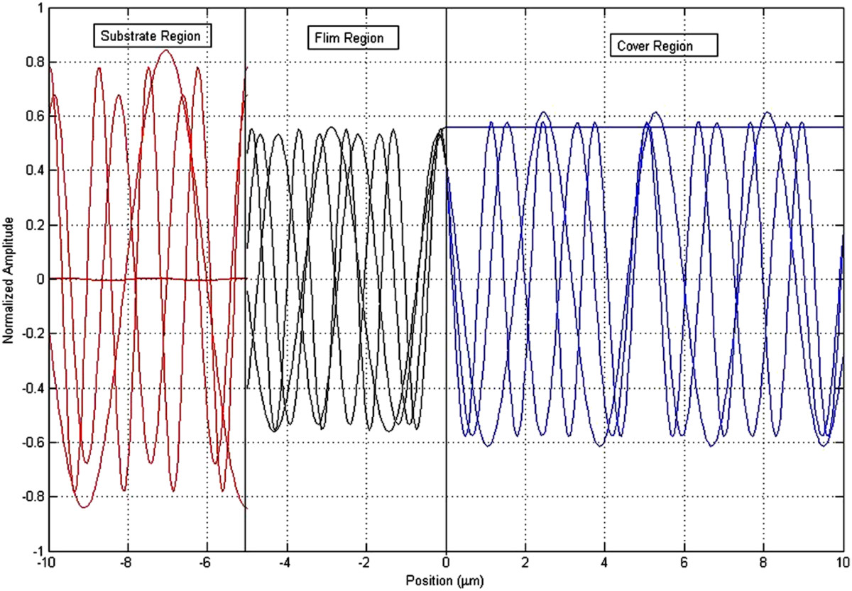
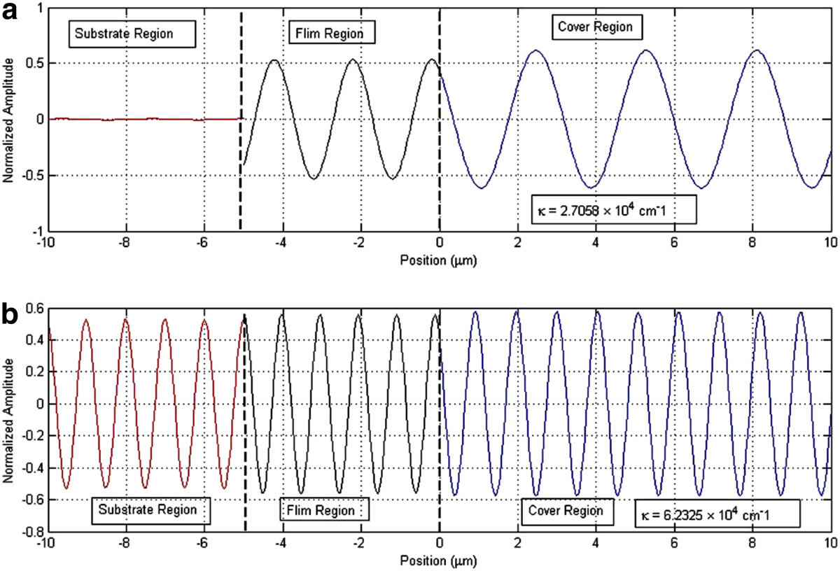
Normalized substrate radiation modes for various values of the transverse wave-vector Elimination and matching of the substrate radiation mode.
(
a
) The substrate radiation mode has been completely eliminated. (
b
) The substrate radiation mode is almost matched with the film regionFigure 1
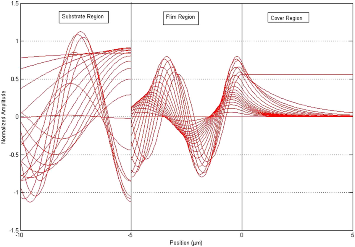
Figure 2

In this case, there is no leakage loss, and practically, it can be used for designing the lossless WDM optical network components. In fact, this particular mode will suffer a lesser amount of leakage loss compared to guided modes. The substrate radiation mode has been perfectly matched while on
Figure
3
shows the mode amplitude difference between the substrate-film interfaces. Hence, computational accuracy has been tested.
Mode amplitude difference versus transverse wave-vector
κ
(cm
−1
)
.Figure 3

The radiation mode is almost perfectly matched at