Advanced Electronic and Nano-Materials Laboratory, Department of Physics, Jamia Millia Islamia, Central University, New Delhi, 110025, IN
Department of Applied Sciences, IEC Engineering College, Greater Noida, 201310, IN
SPECLAB, Department of Physics, University of Puerto Rico, San Juan, PR, 00931, US
Abstract
ZnO is a promising member of the semiconducting materials of II-VI group. ZnO nanocrystals have shown potential applications in various novel technologies. In the present investigation of ZnO nanocrystals, a novel chemical route using Zinc acetate as organic precursor is being reported. ZnO nanocrystals were characterized using X-ray diffraction, scanning electron microscopy UV-visible (UV–vis) spectroscopy, and photoluminescence measurements. The X-ray diffraction studies reveal the typical hexagonal structure of ZnO nanocrystals along the preferred orientation of (101) and (100) planes. The optical bandgap of ZnO nanocrystals was found to be 3.50 eV from the absorbance spectrum, which is higher than that of the bulk ZnO material. A blueshift of 21 nm is observed in the excitonic transitions, which clearly indicates the formation of ZnO nanocrystals. Photoluminescence spectroscopy of the ZnO nanocrystals showed a strong emission peak at 365 nm near the band edge along with a weak green-yellow emission peak spanning the range of 450 to 600 nm. The blueshifting was also observed in the photoluminescence spectrum, in accordance with the UV–vis spectroscopy in contrast to the bulk ZnO material.
Background
Robust ZnO is one of the extensively investigated semiconducting materials of the II-VI group due to its being a promising candidate for technological applications with a wide bandgap of 3.30 eV and large exciton binding energy of about 60 meV[
1
]. ZnO is the only semiconductor material extensively investigated after Si/Ge. Robust ZnO has important applications in the field of biosensors, solar cell window, surface acoustic devices, gas sensor, and piezo actuator devices[
2
,
3
]. Recently, semiconductor nanoparticles have attracted much attention due to their excellent properties like optical, structural, and magnetic. A ZnO nanocluster like nanoparticles, nanobelts, nanorods, nanoflowers, nanowires, nanotubes as well as colloid and bulk nanoparticles also have shown excellent luminescence properties[
4
]. ZnO nanoparticles are not only important for basic research but are also promising for industrial applications at large. Due to the reduction of the grain size, the surface-to-volume ratio increases, which stimulates the discrete nature of the electronic states of the nanomaterials in contrast to the bulk material. Therefore, we may tune the emission wavelengths by altering their grain size. The ZnO nanocrystals have been grown by various methods such as electrodeposition[
5
], pulse laser deposition[
6
], microwave irradiation[
7
], thermal evaporation[
8
], template-assisted growth[
9
], sol–gel route[
10
], etc. However, all the above mentioned techniques need high cost to set up the expensive equipment. Hence, it is still a challenging task to look for simple and cost-effective methods to synthesize metal oxide semiconductor nanoparticles. In the present investigation, we utilized a novel chemical route to synthesize ZnO nanocrystals. However, the sol–gel route is a low-cost, simple synthesis technique that offers control over the size and phase without any expensive equipment[
11
,
12
]. In the present report, we have synthesized the hexagonal-structured ZnO nanocrystals using the zinc acetate organic precursor. The synthesized powder samples have been characterized using X-ray diffraction (XRD), UV-visible (UV–vis) spectroscopy, scanning electron microscopy (SEM), and photoluminescence (PL) spectroscopy. The crystal structure, surface morphology, and optical properties of the fine powders are critically examined.
Methods
In the present work, we have used analytical-grade precursors. All chemicals and reagents were utilized with 99.99% purity from Merck Chemicals (White House Station, NJ, USA) and used without further purification. ZnO nanocrystals were synthesized by the novel chemical route. In this chemical route, we used the inc Acetate [Zn(CH
3
CO
2
)
2
.2H
2
O] precursor as a inc ion source. In this typical synthesis process of ZnO nanocrystals, the inc Acetate was dissolved in NaOH with a molar ratio of 1:85. The solution was strongly stirred with reflux at a constant temperature of 80°C for 3 h; finally, white precipitate was formed within the solution. The solution was filtered by a Whatman filter paper of precise porosity. The precipitate was washed repeatedly many times by ethanol to eliminate impurities. The washed precipitate was annealed at a temperature of 100°C in an oven for 2 h and ground into fine powders. The fine powders were characterized using XRD, SEM, UV–vis, and photoluminescence spectroscopy. The absorbance spectrum of the annealed powders was obtained in the range of 200 to 900 nm using JASCO UV–VIS-NIR spectrometers (Model-V570, Jasco Analytical Instruments, Easton, MD, USA). The structural properties of the synthesized powders were studied using Philips Analytical Diffractometer (Model PW3710, Philips, Amsterdam, Netherlands). The surface morphology of the fine powders was examined using a Zeiss scanning electron microscope (model Carl Zeiss EVO-40, Carl Zeiss AG, Oberkochen, Germany). Photoluminescence spectroscopy of the powder samples was measured using a He-Cd laser as an excitation source, while the sample powders were excited at the 325-nm operating range with an output power of 50 mW, and a Jovin Youvan monochromator (HORIBA, Ltd., Kyoto, Japan) fitted with a Hamamatsu R928 (Hamamatsu, Japan) photomultiplier detector.
Results and discussion
X-ray diffraction analysis
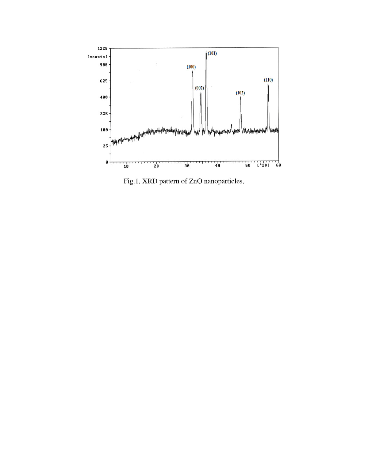
The X-ray diffraction patterns of the synthesized ZnO fine powders are shown in Figure
1
. The X-ray diffraction studies indicated the development of hexagonal structure of the chemically synthesized ZnO nanocrystals. The X-ray pattern peaks are well indexed with JCPDS file number S6314, in agreement with the hexagonal structure of the ZnO nanopowders. The different peak orientations were observed along the (100), (002), (101), (102), and (110) planes. The typical hexagonal wurtzite structure of the synthesized ZnO nanoparticles is inferred from the XRD pattern, which is in good agreement with the intrinsic fundamental structure of ZnO as reported in the literature. The crystallite size (
D
) of the synthesized ZnO nanocrystals was calculated using the Debye-Scherrer formula[
13
] as given below:
D=kλβ2θcosθ
where
k
is a constant taken to be 0.94,
λ
is the wavelength of the X-ray used (
λ
= 1.54 Å),
β2
θ
is the full width at half maxima of the (002) peak of the X-ray diffraction pattern, and 2
θ
is the Bragg angle around 34.44°. Finally, the calculated average value of grain size is found to be 25 nm.
Figure 1
XRD pattern of the ZnO nanoparticles.
SEM analysis
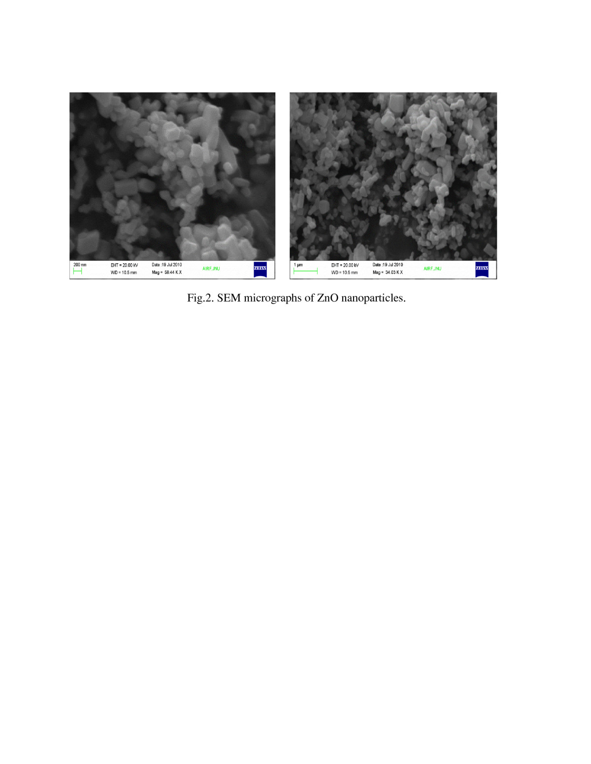
The surface morphology of the synthesized ZnO nanocrystal was examined by SEM micrographs and shown in Figure
2
a,b with magnifications of 58.44 KX and 34.03 KX, respectively. The average grain size of the ZnO nanocrystals observed in the SEM micrographs is of the order of approximately 60 nm. From Figure
2
a,b, it is evident that the SEM micrographs show hexagonal-type structure of the synthesized ZnO nanocrystals. The prominent well-structured growth observed from the SEM micrographs of the fine particles confirms the development of hexagonal wurtzite crystal structure of the ZnO nanocrystals. It may be noted that the grain size of the ZnO fine powders estimated from SEM is in good agreement with the particle size calculated from the XRD analysis[
14
]. The synthesized ZnO powder size investigated was in nanograins; thereby, the increase of surface area ratio with volume plays a vital role in the enhancement of optical properties of the materials. Meanwhile, the reduction of grain size in nanorange confirms the quantum confinement effect to the ZnO powders, which confers as a blueshift due to increase of the bandgap. It is worth mentioning that the optical bandgap of promising application-based materials may be tuned by tailoring its particle size as desired through various novel growth processing techniques. It not only increases the property of the materials but also enhances versatile applicability.
Figure 2
SEM micrographs of ZnO nanoparticles.
With magnifications of (
a
) 58.44 KX and (
b
) 34.03.
Optical properties
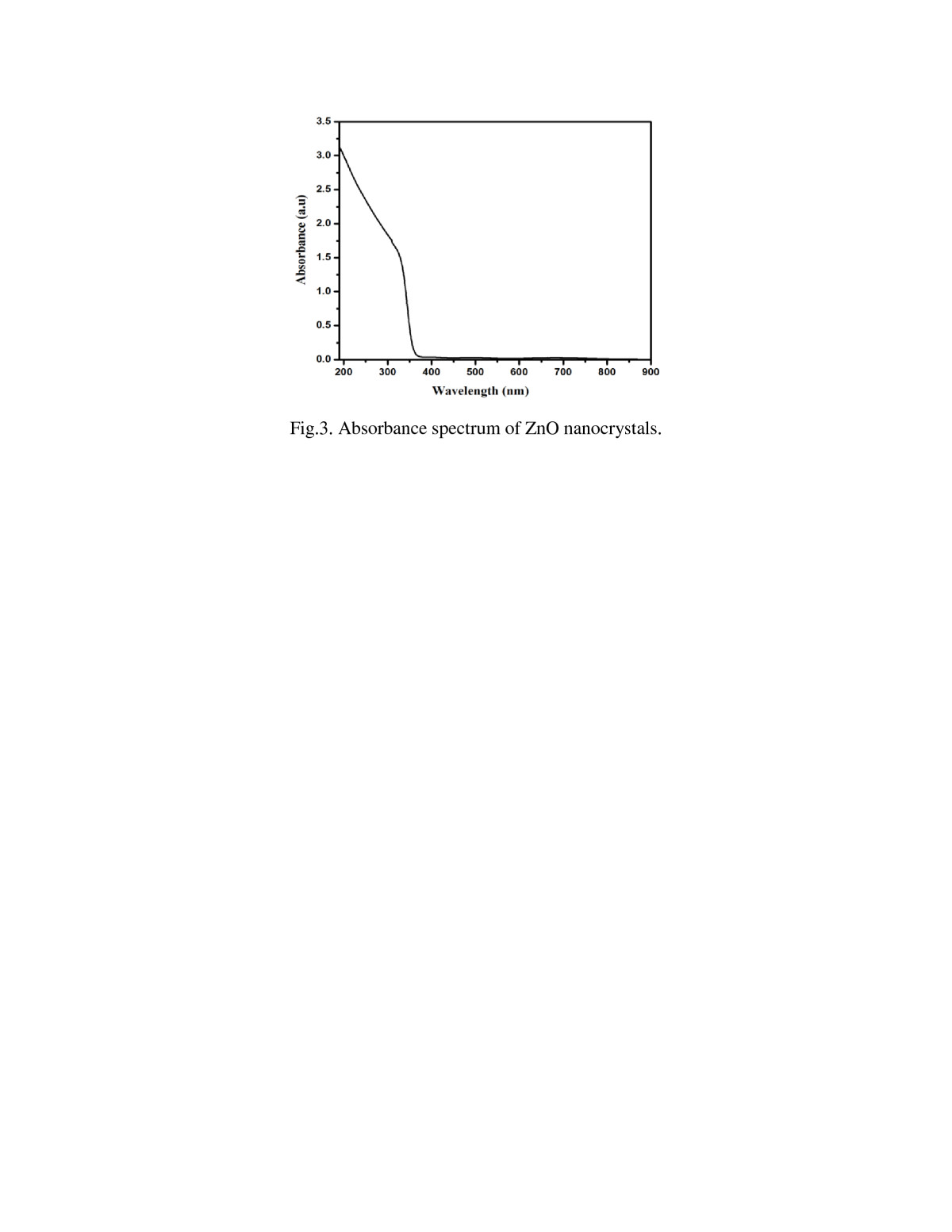
The absorbance spectrum of the synthesized ZnO nanocrystals is shown in Figure
3
. From Figure
3
, it is evident that the ZnO nanocrystals showed high absorbance in the wavelength range of 200 to 270 nm in the absorbance spectrum. The absorbance decreases abruptly near the band edge around 365 nm, after which it turns to the transmittance region. For further confirmation, the particle size of the ZnO nanopowder was also estimated by optical method using the Brus equation[
15
] as given below:
Eeff=Eg+h2π22μR2−1.8e24πɛ'ɛ0R
with (1/μ = 1/
me*
+ 1/
mh*
), where
me*
is the effective mass of the electron (0.19
me
),
mh*
is the effective mass of the hole (0.8
mh
),
R
is the radius of the particle,
ɛ
′ is the dielectric constant (5.7), and
ɛ0
is the permittivity of free space. The particle size of the ZnO nanopowders estimated using the Brus equation was found to be 27 nm, which is in good agreement with the size of 25 nm estimated from the XRD analysis.
Figure 3
Absorbance spectrum of ZnO nanocrystals.
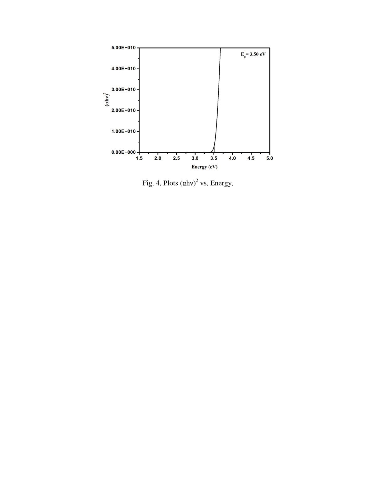
Furthermore, the optical bandgap of the synthesized ZnO nanocrystals was critically examined near the material's fundamental absorption band edge using the Urbach relation given as:
αhν=Ahν−Egm
where
A
is the characteristic parameter (independent of photon energy) for this transition,
h
is Plank's constant, and
ν
is the frequency of the light.
Eg
is the bandgap, and
m
is the parameter which characterizes the transition process involved. The parameter
m
takes the place value of 2 for the direct permitted transition and 1/2 for indirect transitions. The plot of (
αhν
)
2
vs.
hν
for the synthesized ZnO nanocrystals is shown in Figure
4
. The extrapolation of (
αhν
)
2
up to 0 absorption coefficient that intercepts to
hv
provides material bandgap. Hence, the estimated bandgap for the present synthesized ZnO nanopowder material is found to be 3.50 eV, which is more than that of the bulk ZnO material (3.30 eV)[
16
]. It is evident that a blueshift is observed with reference to the bulk ZnO. This study reveals the quantum confinement effect of exciton carriers due to the reduction in ZnO particle size in the range of few nanometers.
Figure 4
Plot of (αhν)2vs. energy.
Photoluminescence
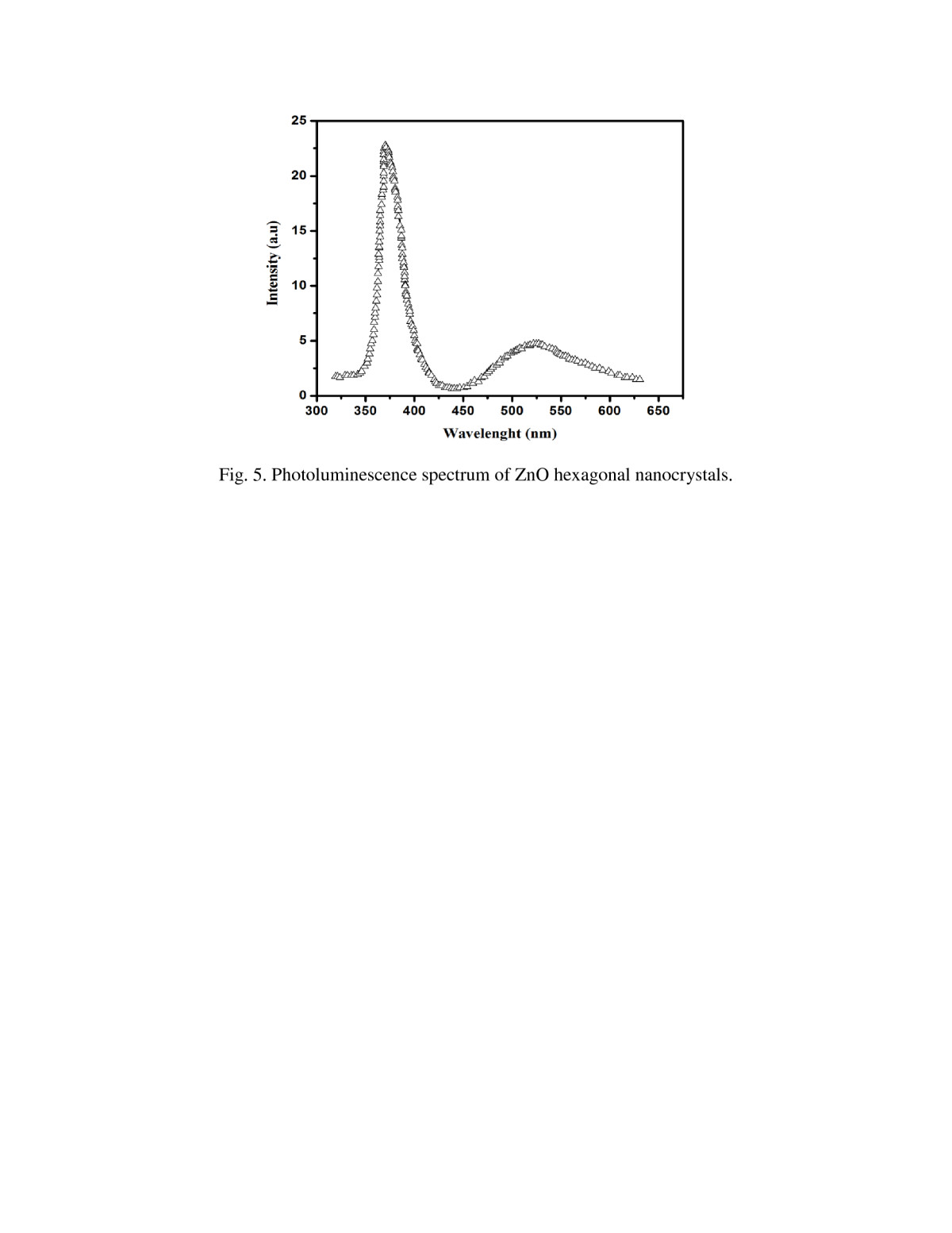
The photoluminescence spectroscopy is an excellent intensive technique for the investigation of the exact band edge transition levels of a material. A well-defined deconvoluted photoluminescence spectrum of the synthesized ZnO nanocrystals is depicted in Figure
5
. The ZnO nanocrystal PL spectrum showed a very strong and intense emission peak at 365 nm, exactly near the band edge emission, while showing no trap-related emission. From the PL study, the optical bandgap of the synthesized ZnO nanoparticles was estimated to be 3.5 eV. The blueshift is also observed in the photoluminescence spectroscopy, consistent with the absorbance spectrum. A broad green-yellow illumination peak is observed over 450 to 600 nm which is attributed to the amount of nonstoichiometry, producing intrinsic defects in the material that may originate from the zinc vacancy and anti-site defect in the ZnO[
17
]. However, it may be noted that localized charge carrier traps within the semiconductor materials are caused by structural defects or chemical impurities. Chemical impurities may also cause a surrounding of structural defects by distorting the lattice as well as the surface of a crystal. The trap states may be caused by the thermal fluctuations of the molecules, which are expected to result in shallow trap states within the bandgap.
Figure 5
Photoluminescence spectrum of ZnO hexagonal nanocrystals.
Conclusions
In the present study, ZnO nanocrystalline powders were synthesized successfully with hexagonal phase through the novel chemical route using inc Acetate as organic precursors. The optical bandgap value of the synthesized ZnO nanocrystals is found to be 3.50 eV from the absorption spectroscopy, while the photoluminescence spectrum reveals a strong emission at 365 nm along with a broad green-yellow emission. In this investigation, a blueshift observed in both of the absorbance optical studies and PL spectroscopy on the ZnO nanoparticles indicates quantum confinement of carriers, which confirms the effective particle size reduction of the synthesized ZnO powders.
Authors’ information
ZRK is working as an assistant professor of Physics in the Department of Applied Sciences, IEC Engineering College, Greater Noida, India. He received his Bachelor and Masters degree in PCM from AMU, Aligrh, India, in 2002 and 2004. In May 2012, he obtained his Ph D degree in the field of material science, optical and structural studies of the semiconducting materials from the Department of Physics, JMI. He has many research papers in peer-review journals in his credit. His current research interest includes fabrication and characterization of II-VI group semiconductor nanocrystalline thin films and their spectroscopic and optoelectronic characterization, synthesis of nanoparticles by chemical routes, especially ZnO and other semiconducting materials, and homogeneous optical waveguide and nonlinear optics. MA is presently associated with Advanced Electronic and Nanomaterials Laboratory at the Department of Physics, Jamia Millia Islamia, Central University. He received his BSc and MSc degrees in 2008 and 2010 from CCS University, Meerut, and the Department of Physics, Jamia Millia Islamia, Central University, New Delhi, India. He is involved with government R&D projects and organizing research lab experiments. His current research interest includes growth and characterization of PZT/ZnO for novel piezoelectric, sensor applications. AS is currently working as an Assistant Professor of Physics at the Department of Physics, Jamia Millia Islamia, Central University. He is engaged in teaching and research with UG, PG, and PhD students. He received his BSc and MSc degrees in 1995 and 1998 from Awdhesh Pratap Singh University, Rewa, India. He obtained his PhD degree in 2005 in the field of material science - processing and characterization of smart materials from the Department of Physics & Astrophysics, University of Delhi, Delhi, India. AS is employed as a research associate at the Department of Physics, University of Delhi since 2003. He moved to the Department of Physics, Jamia Millia Islamia University in 2008. He receives BOYSCAST fellowship of the Government of India to work in the USA on cutting-edge technology. He work as a visiting professor at the University of Puerto Rico, USA. His current research interests are multiferroics, nonmaterials, functional oxides, and photovoltaic energy material.
Acknowledgments
The authors are thankful to the DST, Ministry of Science and Technology, Government of India, and the University Grants Commission, MHRD Government of India for the financial assistant. One of the authors (AS) would like to thank the DST, Ministry of Science and Technology, Government of India for the award of Young Scientist.
Competing interests
The authors declare that they have no competing interests.
Authors’ contributions
ZRK carried out the synthesis and structural properties characterization, participated in the sequence alignment, and drafted the manuscript. MA carried out optical characterization. AS participated in the design of the study and performed the photoluminescence characterization. All authors read and approved the final manuscript" in the Authors’ contributions section.
References
Yan and Chuan-sheng (2009) Synthesis and optical properties of crystalline polymer-capped ZnO nanorods
Shi et al. (2010) Effect of ZnO buffer layer on AZO film properties and photovoltaic applications10.1007/s10856-009-3953-4
Dejene et al. (2011) Optical properties of ZnO nanoparticles by synthesized by varying NaOH concentration
Moghaddam et al. (2009) Synthesis of ZnO nanoparticles and electrodeposition of polypyrrole/ZnO nanocomposites thin films
Unknown ()
Hamedani and Farzaneh (2006) Synthesis of nanocrystals with hexagonal (wurtzite) structure in water using microwave irradiation
Umar et al. (2006) Growth of ZnO nanoneedles on silicon substrate by cyclic feeding chemical vapor deposition: structural and optical properties10.1007/BF02706756
Cao and Liu (2008) Advances in collide and interface
Raja et al. (2008) Preparation of template free zinc oxide nanoparticles using sol–gel chemistry10.1166/jnn.2008.AN24
Singh et al. (2007) Evidence of pseudocubic structure in sol–gel derived Pb1−xCaxTiO3 (x = 0.35–0.48) ceramic by dielectric and Raman spectroscopy10.1063/1.2785843
Singh et al. (2006) Dielectric and piezoelectric properties of sol–gel derived Ca doped PbTiO310.1016/j.mseb.2006.02.055
Khan et al. (2010) Optical and structural properties of thermally evaporated cadmium sulphide thin films on silicon (100) wafers10.1016/j.mseb.2010.03.006
Liu et al. (2009) Synthesis of ZnO hexagonal single-crystal slices with predominant (0001) and (0001) facets by poly(ethylene glycol)-assisted chemical bath deposition10.1021/ja906992s
Khan et al. (2011) Chemical synthesis of CdS nanoparticles and their optical and dielectric studies10.1007/s10853-011-5481-0
Mandal et al. (2008) Photoluminescence and electrical transport characteristics of ZnO nanorods grown by vapor-solid technique10.1016/j.tsf.2008.05.016
Kim et al. (2005) Effect of preheating temperature on structural and optical properties of ZnO thin films by sol–gel process10.1016/j.tsf.2005.06.013